TDA8925 View Datasheet(PDF) - Philips Electronics
Part Name
Description
Manufacturer
TDA8925 Datasheet PDF : 23 Pages
| |||
Philips Semiconductors
Power stage 2 x 15 to 25 W class-D
audio amplifier
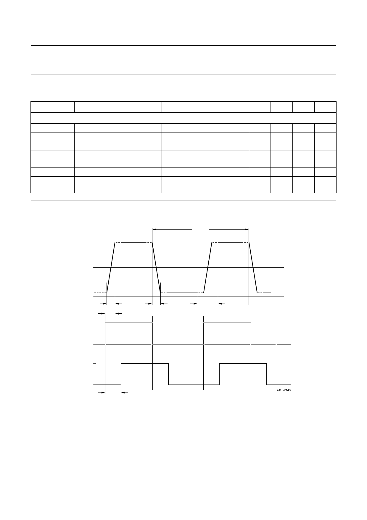
14 SWITCHING CHARACTERISTICS
VP = ±15 V; Tamb = 25 °C; measured in Fig.4; unless otherwise specified.
SYMBOL
PARAMETER
CONDITIONS
PWM outputs (pins OUT1 and OUT2); see Fig.3
tr
tf
tblank
tPD
tW(min)
Rds(on)
rise time
fall time
blanking time
propagation delay
minimum pulse width
on-resistance of the output
transistors
from pin SW1 (SW2) to
pin OUT1 (OUT2)
Product specification
TDA8925
MIN. TYP. MAX. UNIT
−
30
−
ns
−
30
−
ns
−
70
−
ns
−
200 −
ns
−
220 270 ns
−
0.2 0.4 Ω
handbook, full pagewidth
VDD
PWM
output
(V)
0V
VSS
tr
tf
t PD
VSTAB
VSW
(V)
VSS
VSTAB
VREL
(V)
VSS
100 ns
1/ f osc
t blank
MGW145
Fig.3 Timing diagram PWM output, switch and release signals.
2004 May 06
10
Share Link: 