TDA8784 View Datasheet(PDF) - Philips Electronics
Part Name
Description
Manufacturer
TDA8784 Datasheet PDF : 28 Pages
| |||
Philips Semiconductors
18 Msps, 10-bit analog-to-digital
interface for CCD cameras
Product specification
TDA8784
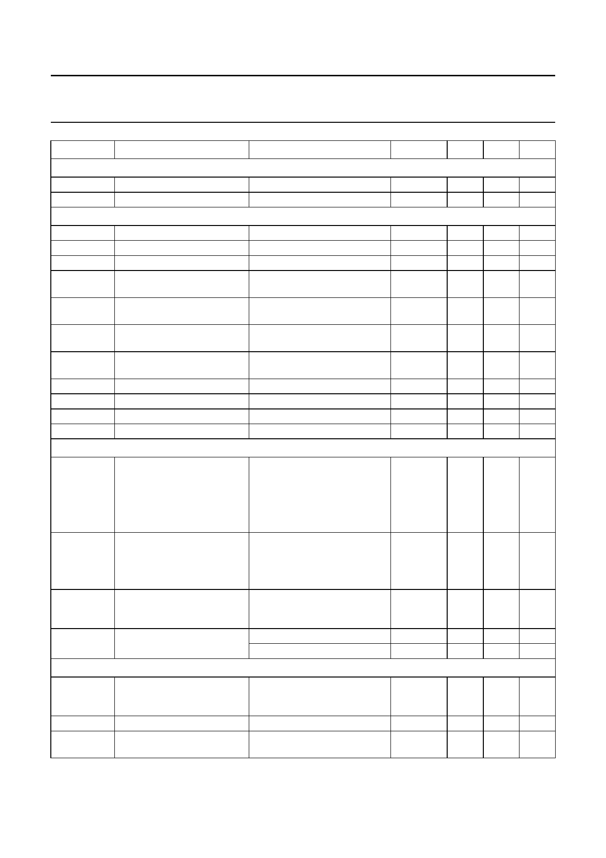
SYMBOL
PARAMETER
CONDITIONS
MIN.
Clamps
gm(ADC)
ADC clamp transconductance at clamp level
−
gm(CDS)
CDS clamp transconductance at clamp level
−
Analog-to-Digital Converter (ADC)
fCLK(max)
maximum clock frequency
18
tCPH
clock pulse width HIGH
15
tCPL
clock pulse width LOW
15
SRCLK
clock input slew rate (rising 10% to 90%
0.5
and falling edge)
Vi(ADC)(p-p) ADC input voltage level
−
(peak-to-peak value)
VRB
ADC reference voltage output
−
code 0
VRT
ADC reference voltage output
−
code 1023
IADCIN
input current pin 10
−2
INL
integral non-linearity
ramp input
−
DNL
differential non-linearity
ramp input
−
td(s)
sampling delay time
−
Total chain characteristics (CDS + AGC + ADC)
td
Ntot(rms)
Voffset(fl-d)
time delay between
SHD and CLK
total output noise (RMS
value)
maximum offset between
CCD floating level and CCD
dark pixel level
see Fig.5; 50% at rising
edges CLK and SHP: transition
full scale code 0 to 1023;
fcut(CDS) = 40 MHz;
fcut(AGC) = 40 MHz;
Vi(CDS) = 1200 mV
fcut(CDS) = 120 MHz;
fcut(AGC) = 40 MHz; note 1
GAGC = 4.5 dB
GAGC = 34.5 dB
−
−
−
−200
Vn(i)(eq)(rms) equivalent input noise voltage AGC gain = 34.5 dB
−
(RMS value)
AGC gain = 4.5 dB
−
Digital-to-analog converter (OFDOUT)
VOFDOUT(p-p) additional 8-bit control DAC
−
(OFD) output voltage
(peak-to-peak value)
VOFDOUT(0) DC output voltage for code 0
−
VOFDOUT(255) DC output voltage for
−
code 255
TYP. MAX. UNIT
7
−
mS
1.5 −
mS
−
−
MHz
−
−
ns
−
−
ns
−
−
V/ns
2
−
V
1.5 −
V
3.5 −
V
−
+120 µA
±0.6 ±1.5 LSB
±0.2 ±0.75 LSB
−
5
ns
40
−
ns
0.125 −
LSB
1.6 −
LSB
−
+200 mV
125 −
µV
150 −
µV
1.4 −
V
2.3 −
V
3.7 −
V
1999 Sep 21
10
Share Link: 