TK65418 View Datasheet(PDF) - Toko America Inc
Part Name
Description
Manufacturer
TK65418 Datasheet PDF : 28 Pages
| |||
TK654xx
ADVANCED INFORMATION
ABSOLUTE MAXIMUM RATINGS
All Pins Except GND ............................................... 6.5 V
Power Dissipation (Note 1) ................................ 400 mW
Storage Temperature Range ................... -55 to +150 °C
Operating Temperature Range ...................-20 to +80 °C
Junction Temperature ........................................... 150 °C
Lead Soldering Temperature (10 s.) ..................... 235 °C
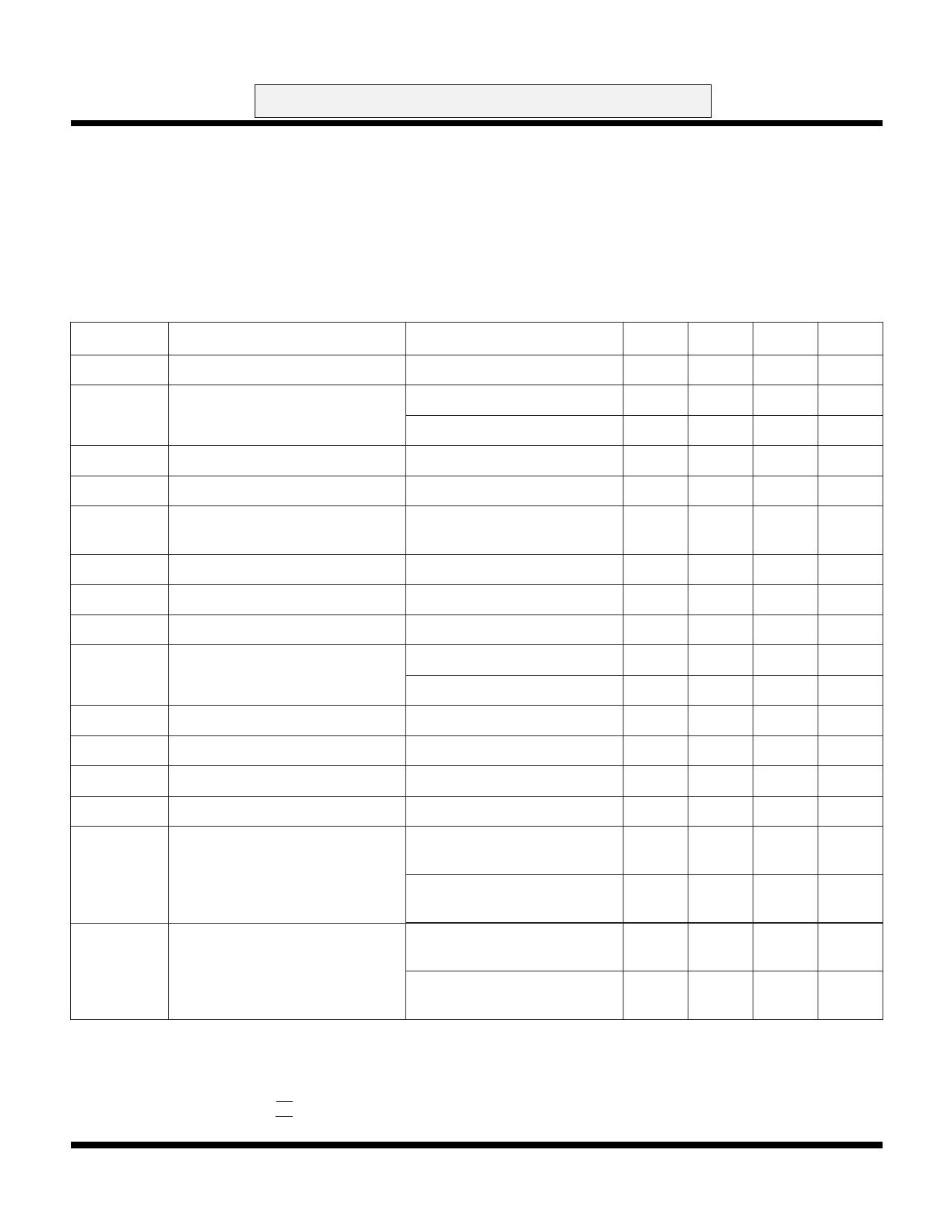
TK654xx ELECTRICAL CHARACTERISTICS
Test conditions: VIN = 5 V, IOUT = 1 mA, TA = TJ = Full Operating Temperature Range, unless otherwise specified.
SYMBOL
PARAMETER
TEST CONDITIONS
MIN TYP MAX UNITS
VIN
VOUT(REG)
Input Voltage
Output Voltage
TA = TJ = 25 ° C (Note 2)
2
6
V
-3%
VREG
3%
V
-5%
+5%
V
∆VOUT(LOAD)
∆VOUT(LINE)
IQ(VOUT)
Load Regulation
Line Regulation
Quiescent Current into VOUT Pin
ILOAD = 0 to 100 mA, (Note 3)
V = 4 to 6 V, (Note 3)
IN
VOUT = VOUT(REG) + 50 mV
(Note 3)
45
6
P 10
120 mV
20
mV
50
µA
I
Q(VIN)
Quiescent Current into V Pin V = V
+ 50 mV
IN
OUT
OUT(REG)
15
65
µA
VTH(LBI)
LBI Input Threshold
TA = TJ = 25 ° C
1.157 1.22 1.282 V
VTH(SB)
Standby Threshold
TA = TJ = 25 ° C
1.157 1.22 1.282 V
IB(SB)
SB Input Bias Current
Note 3
Note 4 at (VTH(SB) - 100 mV)
0
nA
400 720 1000 nA
IOUT(MAX)
Maximum Output Current
(Note 3)
100
mA
IOUT(SC)
Short Circuit Current
(Note 3)
250
mA
IQ(CONV)
Converter Quiescent Current
(Note 3) IOUT = 0 mA
24
90
µA
ISTBY
Converter Standby Current
SB pin = 0 V, Pin 1 open
18
65
µA
EFF
Converter Efficiency
IOUT = 50 mA, (Note 3)
TA = TJ = 25° C (TK65418)
86
91
%
IOUT = 50 mA, (Note 3)
T = T = 25° C (TK65433)
90
95
%
A
J
VDROP
Dropout Voltage
IOUT = 50 mA, (Note 5)
TA = TJ = 25 ° C (TK65418)
IOUT = 50 mA, (Note 6)
TA = TJ = 25 ° C (TK65433)
100 195 mV
75
145 mV
Note 1: Power dissipation is 400 mW when mounted as recommended. Derate at 3.2 mW/°C for operation above 25 °C. Power dissipation is 200
mW in Free Air. Derate at 1.6 mW/°C for operation above 25 °C
Note 2: VREG = 3.3, 3.0, 2.7, 2.5, 2.4, 2.1, 1.8 V.
Note 3: When using test circuit.
Note 4: When using test circuit and ramping VIN down.
Note 5: When using test circuit with SB pin resistors removed and tied to VIN. (VIN = 1.8 V)
Note 6: When using test circuit with SB pin resistors removed and tied to VIN. (VIN = 3.3 V)
Page 2
September 1999 TOKO, Inc.
Share Link: 