HT23C128 View Datasheet(PDF) - Holtek Semiconductor
Part Name
Description
Manufacturer
HT23C128 Datasheet PDF : 8 Pages
| |||
HT23C128
Absolute Maximum Ratings*
Supply Voltage ................................. –0.3V to 6V
Input Voltage........................ –0.3V to VCC+0.3V
Storage Temperature................. –50°C to 125°C
Operating Temperature............... –40°C to 85°C
*Note: These are stress ratings only. Stresses exceeding the range specified under “Absolute Maxi-
mum RatingsвЂқ may cause substantial damage to the device. Functional operation of this
device at other conditions beyond those listed in the specification is not implied and prolonged
exposure to extreme conditions may affect device reliability.
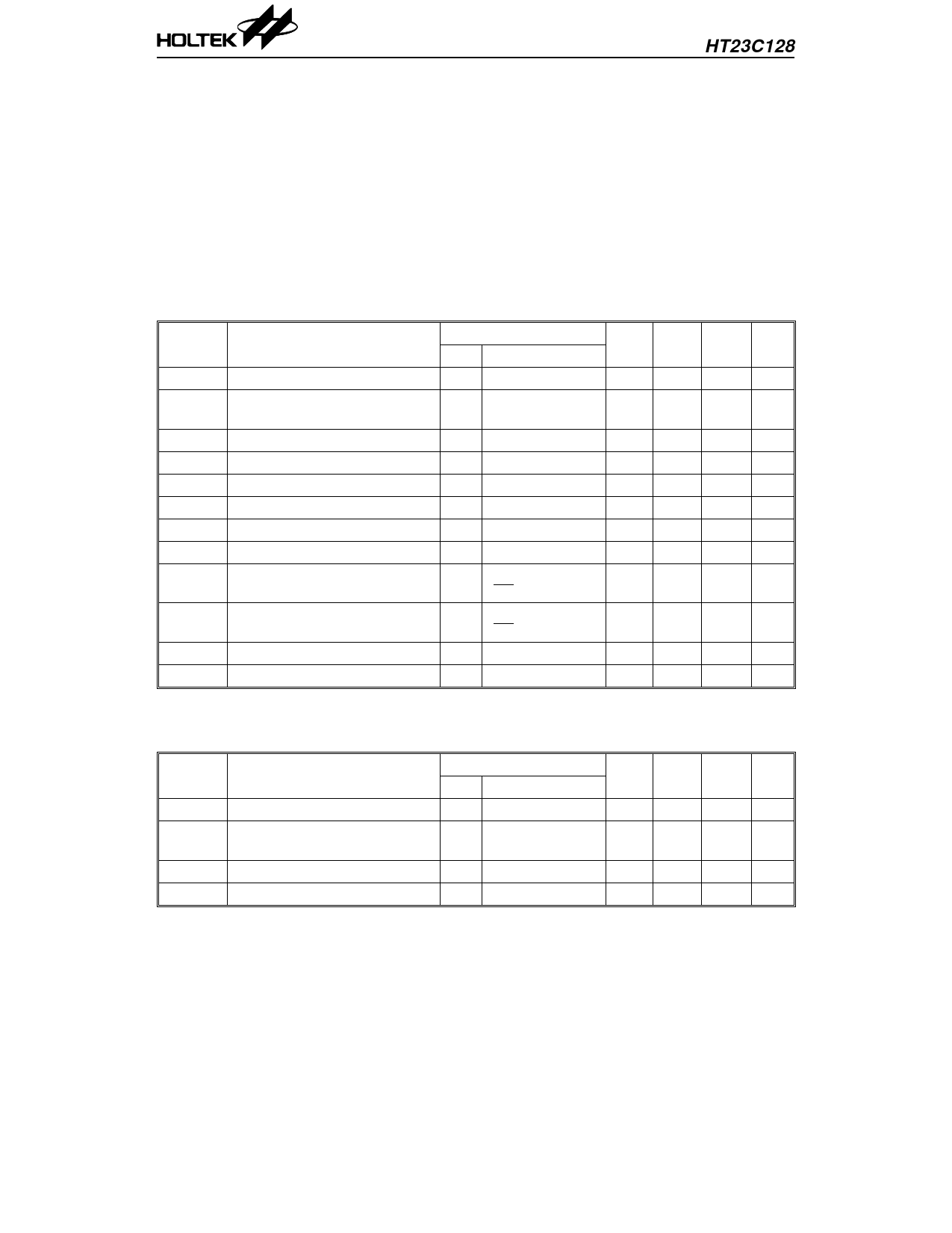
D.C. Characteristics
Supply voltage: 2.7V~3.6V
Ta=–40°C to 85°C
Symbol
Parameter
VCC
ICC
VIL
VIH
VOL
VOH
ILI
ILO
ISTB1
Operating Voltage
Operating Current
Input Low Voltage
Input High Voltage
Output Low Voltage
Output High Voltage
Input Leakage Current
Output Leakage Current
Standby Current
ISTB2
CIN
COUT
Standby Current
Input Capacitance (See note)
Output Capacitance (See note)
Test Conditions
VCC Conditions
—
—
3V
O/P Unload,
f=5MHz
3V
—
3V
—
3V IOL=2.1mA
3V IOH=–0.4mA
3V VIN=0 to VCC
3V VOUT=0 to VCC
3V
CE=VIL
CE=VIH
3V
CE≤0.2V
CEв‰ӨVCC-0.2V
— f=1MHz
— f=1MHz
Min. Typ. Max. Unit
2.7 — 3.6 V
— — 10 mA
VSS — 0.4 V
2.0 — VCC V
— — 0.4 V
2.4 — VCC V
—
—
10 ВµA
—
—
10 ВµA
— — 500 µA
—
—
10 ВµA
— — 10 pF
— — 10 pF
Note: These parameters are periodically sampled but not 100% tested.
Supply voltage: 4.5V~5.5V
Symbol
Parameter
VCC
Operating Voltage
ICC
Operating Current
VIL
Input Low Voltage
VIH
Input High Voltage
Test Conditions
VCC Conditions
—
—
5V
O/P Unload,
f=5MHz
5V
—
5V
—
Ta=–40°C to 85°C
Min. Typ. Max. Unit
4.5 — 5.5 V
— — 25 mA
VSS — 0.8 V
2.2 — VCC V
3
24th Aug ’98
Share Link: 