CDP1805AC View Datasheet(PDF) - Intersil
Part Name
Description
Manufacturer
CDP1805AC Datasheet PDF : 30 Pages
| |||

CDP1805AC, CDP1806AC
MA0 to MA7 (8 Memory Address Lines)
ME (Memory Enable CDP1805AC Only)
In each cycle, the higher-order byte of a 16-bit memory
address appears on the memory address lines MA0-7 first.
Those bits required by the memory system can be strobed
into external address latches by timing pulse TPA. The low-
order byte of the 16-bit address appears on the address
lines 1/2 clock after the termination of TPA.
MWR (Write Pulse)
A negative pulse appearing in a memory-write cycle, after
the address lines have stabilized.
MRD (Read Level)
A low level on MRD indicates a memory read cycle. It can be
used to control three-state outputs from the addressed mem-
ory and to indicate the direction of data transfer during an I/O
instruction.
This active low input is used to select or deselect the internal
RAM. It must be active prior to clock 70 for an internal RAM
access to take place. Internal RAM data will appear on the
data bus during the time that ME is active (after clock 31).
Thus, if this data is to be latched into an external device (i.e.,
during an OUTPUT instruction or DMA OUT cycle), ME
should be wide enough to provide enough time for valid data
to be latched. The internal RAM is automatically deselected
after clock 71. ME is ineffective when MRD • MWR = 1.
The internal RAM is not internally mask-decoded. Decoding
of the starting address is performed externally, and may
reside in any 64-byte block of memory.
VDD (CDP1806AC Only)
This input replaces the ME signal of the CDP1805AC and
must be connected to the positive power supply.
Q
Single bit output from the CPU which can be set or reset,
under program control. During SEQ and REQ instruction
execution, Q is set or reset between the trailing edge of TPA
and the leading edge of TPB. The Q line can also be con-
trolled by the Counter/Timer underflow via the Enable Toggle
Q instruction.
The Enable Toggle Q command connects the Q-line flip-flop
to the output of the counter, such that each time the counter
decrements from 01 to its next value, the Q line changes
state. This command is cleared by a LOAD COUNTER
(LDC) instruction with the Counter/Timer stopped, a CPU
reset, or a BRANCH COUNTER INTERRUPT (BCl) instruc-
tion with the counter interrupt flip-flop set.
Clock
Input for externally generated single-phase clock. The maxi-
mum clock frequency is 5MHz at VDD = 5V. The clock is
counted down internally to 8 clock pulses per machine cycle.
XTAL
Connection to be used with clock input terminal, for an exter-
nal crystal, if the on-chip oscillator is utilized.
VDD, VSS, (Power Levels)
VSS is the most negative supply voltage terminal and is nor-
mally connected to ground. VDD is the positive supply volt-
age terminal. All outputs swing from VSS to VDD. The
recommended input voltage swing is from VSS to VDD.
Architecture
Figure 2 shows a block diagram of the CDP1805AC and
CDP1806AC. The principal feature of this system is a regis-
ter array (R) consisting of sixteen 16-bit scratchpad regis-
ters. Individual registers in the array (R) are designated
(selected) by a 4-bit binary code from one of the 4-bit regis-
ters labeled N, P, and X. The contents of any register can be
directed to any one of the following paths:
1. The external memory (multiplexed, higher-order byte first
on to 8 memory address lines).
2. The D register (either of the two bytes can be gated to D).
3. The increment/decrement circuit where it is increased or
decreased by one and stored back in the selected 16-bit
register.
4. To any other 16-bit scratch pad register in the array.
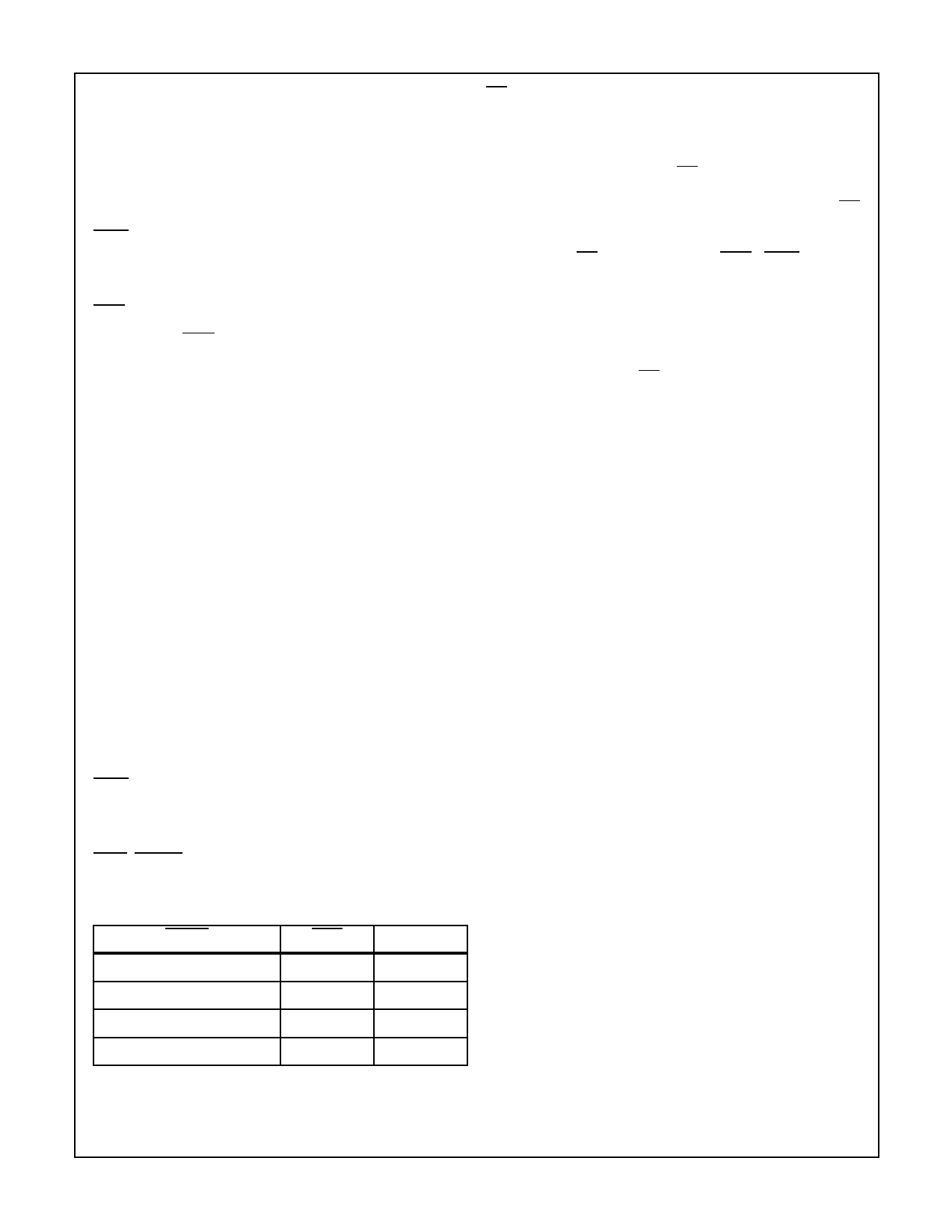
WAIT, CLEAR (2 Control Lines)
Provide four control modes as listed in the following truth
table:
CLEAR
L
L
WAIT
L
H
MODE
Not Allowed
Reset
H
L
Pause
H
H
Run
The four paths, depending on the nature of the instruction,
may operate independently or in various combinations in the
same machine cycle.
Most instructions consist of two 8-clock-pulse machine
cycles. The first cycle is the fetch cycle, and the second, and
more if necessary, are execute cycles. During the fetch cycle
the four bits in the P designator select one of the 16 registers
R(P) as the current program counter. The selected register
R(P) contains the address of the memory location from
which the instruction is to be fetched. When the instruction is
read out from the memory, the higher order 4 bits of the
instruction byte are loaded into the register and the lower
order 4 bits into the N register. The content of the program
counter is automatically incremented by one so that R(P) is
now “pointing” to the next byte in the memory.
10