CDP1805AC View Datasheet(PDF) - Intersil
Part Name
Description
Manufacturer
CDP1805AC Datasheet PDF : 30 Pages
| |||
CDP1805AC, CDP1806AC
Absolute Maximum Ratings
DC Supply Voltage Range, (VDD)
(All Voltages Referenced to VSS Terminal). . . . . . . . . -0.5V to +7V
Input Voltage Range, All Inputs . . . . . . . . . . . . . -0.5V to VDD +0.5V
DC Input Current, any One Input . . . . . . . . . . . . . . . . . . . . . . . . . ±10mA
Thermal Information
Thermal Resistance (Typical, Note 2)
θJA (oC/W) θJC (oC/W)
PDIP Package . . . . . . . . . . . . . . . . . . .
50
N/A
PLCC Package . . . . . . . . . . . . . . . . . .
46
N/A
SBDIP Package. . . . . . . . . . . . . . . . . .
55
15
Device Dissipation Per Output Transistor
TA = Full Package Temperature Range . . . . . . . . . . . . . . 100mW
Operating Temperature
Package Type D . . .
Range
......
(TA)
....
.
.
.
.
.
.
.
.
.
.
.
. -55oC
to
+125oC
Package Type E and Q . . . . . . . . . . . . . . . . . . . . .-40oC to +85oC
Storage Temperature Range (TSTG). . . . . . . . . . . .-65oC to +150oC
Lead Temperature (During Soldering)
At Distance 1/16 ±1/32in (1.59 ± 0.79mm) from case for
10s Max . . . . . . . . . . . . . . . . . . . . . . . . . . . . . . . . . . . . . . +265oC
Printed Circuit Board Mount: 57mm x 57mm Minimum Area x 1.6mm
Thick G10 Epoxy Glass, or Equivalent.
CAUTION: Stresses above those listed in “Absolute Maximum Ratings” may cause permanent damage to the device. This is a stress only rating and operation
of the device at these or any other conditions above those indicated in the operational sections of this specification is not implied.
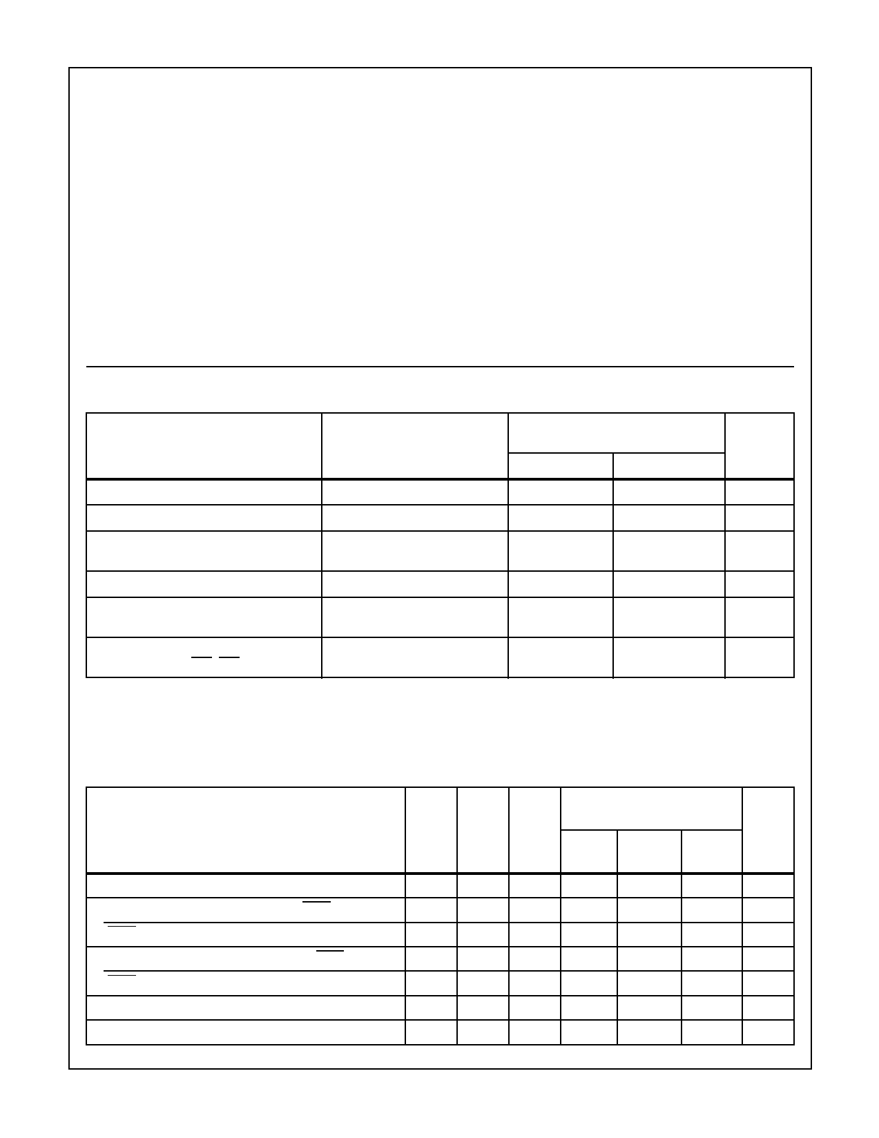
Recommended Operating Conditions TA = Full-Package Temperature Range. For maximum reliability, operating conditions
should be selected so that operation is always within the following ranges.
PARAMETER
TEST CONDITIONS
VDD
(V)
CDP1805ACD, CDP1805ACE
CDP1806ACD, CDP1806ACE
MIN
MAX
UNITS
DC Operating Voltage Range
-
4
6.5
V
Input Voltage Range
Minimum Instruction Time (Note 1)
(fCL = 5MHz)
Maximum DMA Transfer Rate
-
VSS
VDD
V
5
3.2
-
µs
5
-
0.625
Mbyte/s
Maximum Clock Input Frequency,
5
Load Capacitance (CL) = 50pF
Maximum External Counter/Timer Clock
5
Input Frequency to EF1, EF2
DC
5
MHz
DC
2
MHz
NOTES:
1. Equals 2 machine cycles - one Fetch and one Execute operation for all instructions except Long Branch, Long Skip, NOP, and “68” family
instructions, which are more than two cycles.
2. θJA is measured with the component mounted on an evaluation PC board in free air.
Static Electrical Specifications at TA = -40oC to +85oC, VDD ±5%, Except as Noted
CDP1805ACD, CDP1805ACE
CDP1806ACD, CDP1806ACE
PARAMETER
VO
VIN
VDD
(NOTE 3)
(V)
(V)
(V)
MIN
TYP
MAX UNITS
Quiescent Device Current, IDD
Output Low Drive (Sink) Current, (Except XTAL), IOL
XTAL Output, IOL
Output High Drive (Source) Current (Except XTAL, IOH
XTAL, IOH
Output Voltage Low Level, VOL
Output Voltage High Level, VOH
-
0, 5
5
-
50
0.4
0, 5
5
1.6
4
0.4
5
5
0.2
0.4
4.6
0, 5
5
-1.6
-4
4.6
0
5
-0.1
-0.2
-
0, 5
5
-
0
-
0, 5
5
4.9
5
200
µA
-
mA
-
mA
-
mA
-
mA
0.1
V
-
V
4
Share Link: 