CDP1805AC View Datasheet(PDF) - Intersil
Part Name
Description
Manufacturer
CDP1805AC Datasheet PDF : 30 Pages
| |||
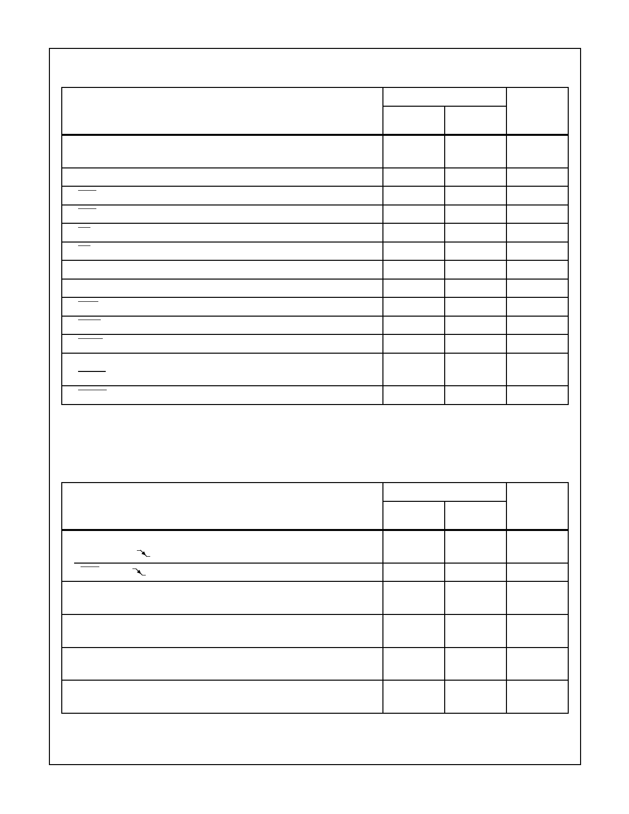
CDP1805AC, CDP1806AC
Dynamic Electrical Specifications at TA = -40o to +85oC; C L = 50pF; Input tR, tF = 10ns; Input Pulse Levels = 0.1V to
VDD -0.1V; VDD = 5V, ±5%. (Continued)
CDP1805AC CDP1806AC
PARAMETER
(NOTE 5)
TYP
MAX
UNITS
Minimum Set-Up And Hold Times (Note 2)
Data Bus Input Set-Up, tSU
-100
0
ns
Data Bus Input Hold, tH
125
225
ns
DMA Set-Up, tSU
-75
0
ns
DMA Hold, tH
100
175
ns
ME Set-Up, t
SU
ME Hold, tH
125
320
ns
0
50
ns
Interrupt Set-Up, tSU
-100
0
ns
Interrupt Hold, tH
100
175
ns
WAIT Set-Up, tSU
20
50
ns
EF1-4 Set-Up, tSU
-125
0
ns
EF1 -4 Hold, tH
175
300
ns
Minimum Pulse Width Times (Note 6)
CLEAR Pulse Width, tWL
100
175
ns
CLOCK Pulse Width, tW
75
100
ns
NOTES:
5. Typical values are for TA = 25o C and nominal VDD.
6. Maximum limits of minimum characteristics are the values above which all devices function.
Timing Specifications as a function of T (T = 1/fCLOCK) at TA = -40 to +85oC, VDD = 5V, ±15%
CDP1805AC, CDP1806AC
PARAMETER
(NOTE 7)
TYP
MAX
High-Order Memory-Address Byte
Set-Up to TPA
Time, tSU
MRD to TPA
Time, tSU
High-Order Memory-Address Byte
Hold after TPA Time, tH
Low-Order Memory-Address Byte
Hold after WR Time, tH
CPU Data to Bus
Hold after WR Time, tH
Required Memory Access Time, tACC
Address to Data
2T-275
T/2 -100
2T -175
T/2 -75
T/2 +75
T/2 +100
T +180
T +240
T +110
T +150
4.5T -440
4.5T -330
NOTE:
7. Typical values are for TA = +25oC and nominal VDD.
UNITS
ns
ns
ns
ns
ns
ns
6
Share Link: 