CDP1805AC View Datasheet(PDF) - Intersil
Part Name
Description
Manufacturer
CDP1805AC Datasheet PDF : 30 Pages
| |||
CDP1805AC, CDP1806AC
Enhanced CDP1805AC and CDP1806AC
Operation
MRD = VDD: Input data from I/O to CPU and memory.
MRD = VSS: Output data from Memory to I/O.
Timing
EF1 to EF4 (4 Flags)
Timing for the CDP1805AC and CDP1806AC is the same as
the CDP1802 microprocessor series, with the following
exceptions:
• 4.5 Clock Cycles Are Provided for Memory Access Instead
of 5.
• Q Changes 1/2 Clock Cycle Earlier During the SEQ and
REQ Instructions.
These inputs enable the I/O controllers to transfer status
information to the processor. The levels can be tested by the
conditional branch instructions. They can be used in con-
junction with the INTERRUPT request line to establish inter-
rupt priorities. The flag(s) are sampled at the end of every S0
cycle. EF1 and EF2 are also used for event counting and
pulse width measurement in conjunction with the
Counter/Timer.
• Flag Lines (EF1-EF4) Are Sampled at the End of the S0
Cycle Instead of at the Beginning of the S1 Cycle.
• Pause Can Only Occur on the Low-To-High Transition of
Either TPA or TPB, Instead of any Negative Clock Transi-
tion.
Special Features
Schmitt triggers are provided on all inputs, except ME and
BUS 0-BUS 7, for maximum immunity from noise and slow
signal transitions. A Schmitt Trigger in the oscillator section
allows operation with an RC or crystal.
The CDP1802 Series LOAD mode is not retained. This
mode (WAIT, CLEAR = 0) is not allowed on the CDP1805AC
and CDP1806AC.
A low power mode is provided, which is initiated via the IDLE
instruction. In this mode all external signals, except the oscil-
lator, are stopped on the low-to-high transition of TPB. All
outputs remain in their previous states, MRD is set to a logic
“1”, and the data bus floats. The IDLE mode is exited by a
DMA or INT condition. The INT includes both external inter-
rupts and interrupts generated by the Counter/Timer. The
only restrictions are that the Timer mode, which uses the
TPA ÷ 32 clock source, and the underflow condition of the
Pulse Width Measurement modes are not available to exit
the IDLE mode.
INTERRUPT, DMA-IN, DMA-OUT (3 I/O Requests)
DMA-lN and DMA-OUT are sampled during TPB every S1,
S2, and S3 cycle. INTERRUPT is sampled during TPB every
S1 and S2 cycle.
Interrupt Action - X and P are stored in T after executing
current instruction; designator X is set to 2; designator P is
set to 1; interrupt enable (MIE) is reset to 0 (inhibit); and
instruction execution is resumed. The interrupt action
requires one machine cycle (S3).
DMA Action - Finish executing current instruction; R(0)
points to memory area for data transfer; data is loaded into
or read out of memory; and R(0) is incremented.
NOTE: In the event of concurrent DMA and INTERRUPT requests,
DMA-IN has priority followed by DMA-OUT and then INTERRUPT.
(The interrupt request is not internally latched and must be held true
after DMA).
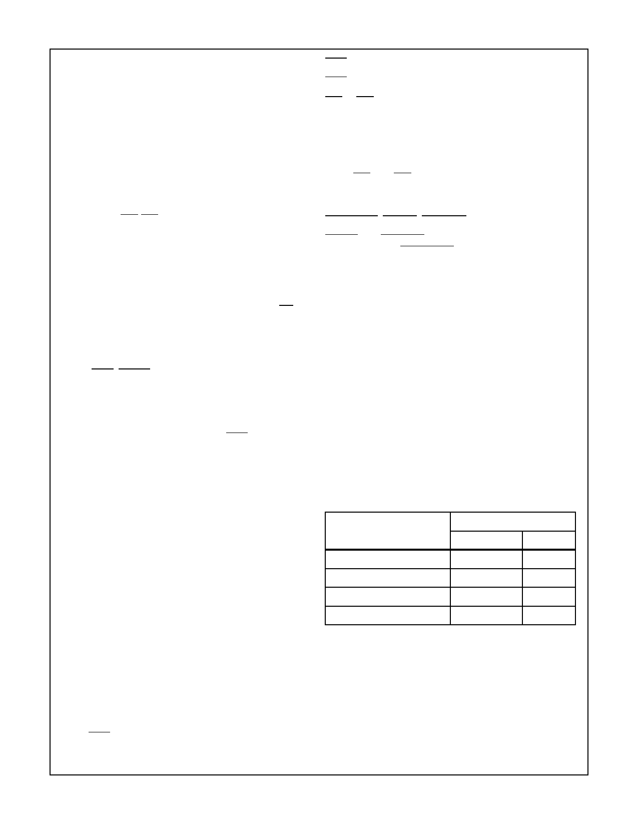
SC0, SC1, (2 State Code Lines)
These outputs indicate that the CPU is: 1) fetching an
instruction, or 2) executing an instruction, or 3) processing a
DMA request, or 4) acknowledging an interrupt request. The
levels of state code are tabulated below. All states are valid
at TPA.
STATE CODE LINES
Signal Descriptions
Bus 0 to Bus 7 (Data Bus)
8-Bit bidirectional DATA BUS lines. These lines are used for
transferring data between the memory, the microprocessor,
and I/O devices.
N0 to N2 (I/O) Lines
Activated by an I/O instruction to signal the I/O control logic
of a data transfer between memory and I/O interface. These
lines can be used to issue command codes or device selec-
tion codes to the I/O devices. The N-bits are low at all times
except when an I/O instruction is being executed. During this
time their state is the same as the corresponding bits in the
N Register. The direction of data flow is defined in the I/O
instruction by bit N3 (internally) and is indicated by the level
of the MRD Signal:
STATE TYPE
SC1
SC0
S0 (Fetch)
L
L
S1 (Execute)
L
H
S2 (DMA)
H
L
S3 (Interrupt)
H
H
NOTE: H = VDD, L = VSS.
TPA, TPB (2 Timing Pulses)
Positive pulses that occurrence in each machine cycle (TPB
follows TPA). They are used by I/O controllers to interpret
codes and to time interaction with the data bus. The trailing
edge of TPA is used by the memory system to latch the high-
order byte of the multiplexed 16-bit memory address.
9
Share Link: 