CDP1878C View Datasheet(PDF) - Intersil
Part Name
Description
Manufacturer
CDP1878C Datasheet PDF : 13 Pages
| |||
CDP1878C
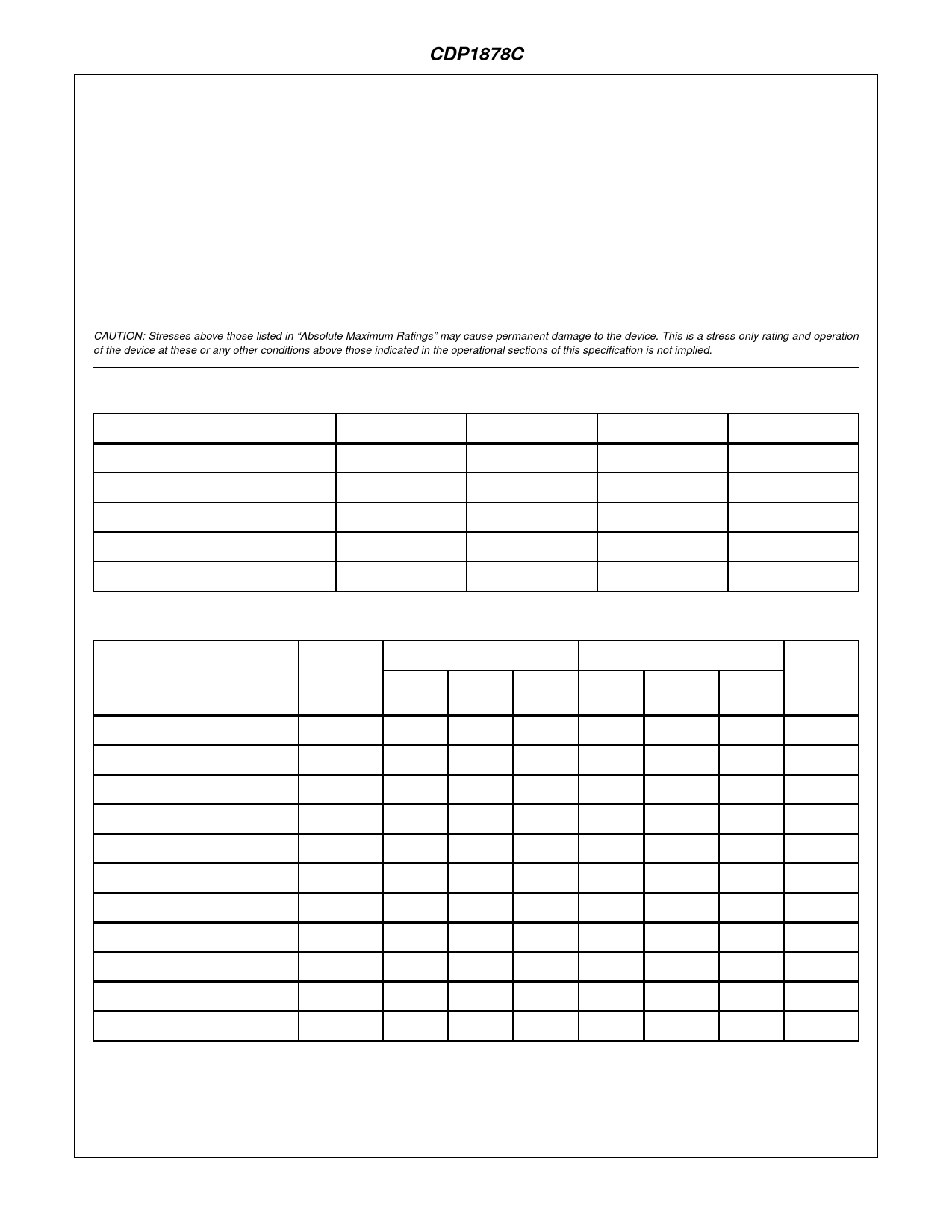
Absolute Maximum Ratings
Thermal Information
DC Supply-Voltage Range, (VDD)
(All Voltages Referenced to VSS Terminal)
CDP1878C . . . . . . . . . . . . . . . . . . . . . . . . . . . . . . . . . -0.5V to +7V
Input Voltage Range, All Inputs . . . . . . . . . . . . . -0.5V to VDD +0.5V
DC Input Current, Any One Input. . . . . . . . . . . . . . . . . . . . . . . . .±10mA
Thermal Resistance (Typical)
θJA (oC/W) θJC (oC/W)
PDIP Package . . . . . . . . . . . . . . . . . . .
55
N/A
SBDIP Package . . . . . . . . . . . . . . . . . .
50
12
Device Dissipation Per Output Transistor
TA = Full Package Temperature Range
(All Package Types) . . . . . . . . . . . . . . . . . . . . . . . . . . . . . . 100mW
Operating Temperature Range (TA)
Package Type D. . . . . . . . . . . . . . . . . . . . . . . . . .-55oC to +125oC
Package Type E . . . . . . . . . . . . . . . . . . . . . . . . . . .-40oC to +85oC
Storage Temperature Range (TSTG). . . . . . . . . . . .-65oC to +150oC
Lead Temperature (During Soldering)
At distance 1/16 ± 1/32 In. (1.59 ± 0.79mm)
from case for 10s max . . . . . . . . . . . . . . . . . . . . . . . . . . . . +265oC
CAUTION: Stresses above those listed in “Absolute Maximum Ratings” may cause permanent damage to the device. This is a stress only rating and operation
of the device at these or any other conditions above those indicated in the operational sections of this specification is not implied.
Recommended Operating Conditions At TA = Full Package Temperature Range. For maximum reliability, operating conditions
should be selected so that operation is always within the following ranges:
PARAMETER
SYMBOL
MIN
MAX
UNITS
DC Operating Voltage Range
4
6.5
V
Input Voltage Range
VSS
Maximum Clock Input Rise or Fall Time
tR, tF
-
Minimum Clock Pulse Width
tWL, tWH
200
Maximum Clock Input Frequency
fCL
DC
VDD
5
-
1
V
µs
ns
MHz
Static Electrical Specifications At TA = -40oC to +85oC, VDD ± 5% Except as noted:
CONDITIONS
LIMITS
PARAMETER
VO
SYMBOL
(V)
VIN
VDD
(NOTE 1)
(V)
(V)
MIN
TYP
MAX
UNITS
Quiescent Device Current
IDD
-
0, 5
5
-
0.02
200
µA
Output Low Drive (Sink) Current
IOL
0.4
0, 5
5
1.6
3.2
-
mA
Output High Drive (Source) Current
IOH
4.6
0, 5
5
-1.15
-2.3
-
mA
Output Voltage Low-Level (Note 2)
VOL
-
0, 5
5
-
0
0.1
V
Output Voltage High-Level (Note 2)
VOH
-
0, 5
5
4.9
5
-
V
Input Low Voltage
VIL
0.5, 4.5
-
5
-
-
1.5
V
Input High Voltage
VIH
0.5, 9.5
-
5
3.5
-
-
V
Input Leakage Current
IIN
Any Input 0, 5
5
-
-
±1
µA
Operating Current (Note 3)
IDD1
-
0, 5
5
-
1.5
3
mA
Input Capacitance
CIN
-
-
-
-
5
7.5
pF
Output Capacitance
COUT
-
-
-
-
10
15
pF
NOTES:
1. Typical values are for TA = +25oC and nominal VDD.
2. IOL = IOH = 1µA
3. Operating current measured at 200kHz for VDD = 5V, with open outputs (worst-case frequencies for CDP1802A system operating at max-
imum speed of 3.2MHz).
4-92
Share Link: 