CDP1878C View Datasheet(PDF) - Intersil
Part Name
Description
Manufacturer
CDP1878C Datasheet PDF : 13 Pages
| |||
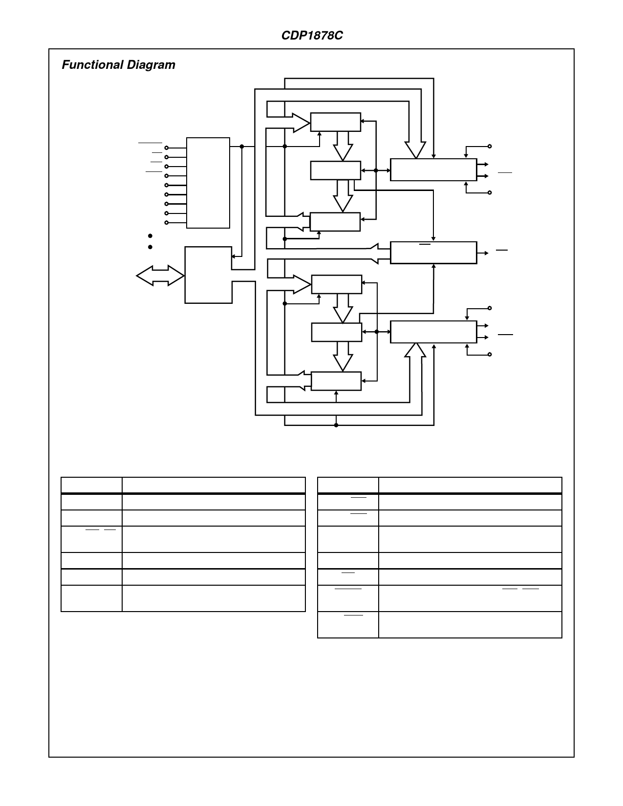
Functional Diagram
RESET
RD
TPB/WR
IO/MEM
TPA
CS
A2
A1
A0
VDD
VSS
8-BIT
EXTERNAL
BUS
I-O
CONTROL
AND
LOGIC
DATA
BUS
DRIVERS
CDP1878C
JAM
REGISTER A
COUNTER A
HOLDING
REGISTER A
JAM
REGISTER B
COUNTER B
HOLDING
REGISTER B
CONTROL REGISTER A
AND MODE CONTROL
GATE A
TAO
TAO
CLOCK A
INT AND
STATUS REGISTER
INT
CONTROL REGISTER B
AND MODE CONTROL
GATE B
TBO
TBO
CLOCK B
FUNCTIONAL DEFINITIONS FOR CDP1878C TERMINALS
TERMINAL
USAGE
VDD - VSS
DB0-DB7
Power
Data to and from device
TPB/WR, RD Directional Control Signals
A0, A1, A2 Addresses that select counters or registers
TACL, TBCL Clocks used to decrement counters
TAG, TBG Gate inputs that control counters
TERMINAL
TAO, TAO
TBO, TBO
TPA
CS
INT
RESET
IO/MEM
USAGE
Complemented outputs of Timer A
Complemented outputs of Timer B
Used with CDP1800-series processors, tied high
otherwise
Active high input that enables device
Low when counter is “0”
When active, TAO, TBO are low, TAO, TBO are
high. Interrupt status register is cleared.
Tied high in CDP1800 input/output mode, other-
wise tied low
4-93
Share Link: 