CDP1878C View Datasheet(PDF) - Intersil
Part Name
Description
Manufacturer
CDP1878C Datasheet PDF : 13 Pages
| |||
CDP1878C
Functional DescriptIon
The dual counter-timer consists of two programmable 16-bit
down counters, separately addressable and controlled by
two independent 8-bit control registers. The word in the con-
trol register determines the mode and type of operation that
the counter-timer performs. Writing to or reading from a
counter or register is enabled by selective addressing during
a write or read cycle. The data is placed on the data bus by
the microprocessor during the write cycle or read from the
counter during the read cycle. Data to and from the counters
and to the control registers is in binary format.
Each counter-timer consists of three parts. The first is the
counter itself, a 16-bit down counter that is decremented on
the trailing edge of the clock input. The second is the jam
register that receives the data when the counter is written to.
The word in the control register determines when the jam
register value is placed into the counter. The third part is the
holding register that places the counter value on the data
bus when the counter is read.
When the counter has decremented to zero, three events
occur. The first involves the common interrupt output pin that,
if enabled, becomes active low. The second is the setting of a
bit in the interrupt status register. This register can be read to
determine which counter-timer has timed out. The third event
is the logic change of the complemented output pins.
In addition to the clock input used to decrement the counter, a
gate input is available to enable or initiate operation. The
counter-timers are independent and can have different mode
operations.
Write Operation
The counters and registers are separately addressable and
are programmed via the data bus when the chip is selected
with the TPB/WR pin active. Normal sequencing requires that
the counter jam register be loaded first with the required value
(most significant and least significant byte in any order), and
then the control register be accessed and loaded with the
control word. The trailing edge of the TPB/WR pulse will latch
the control word into the control register. The trailing edge of
the first clock to occur with gate valid will cause the counter to
be jammed with its initial value. The counter will decrement on
the trailing edge of succeeding clocks as long as the gate is
valid, until it reaches zero. The output levels will then change,
and if enabled, the interrupt output will become active and the
appropriate timer bit will be set in the interrupt status register.
The interrupt output and the interrupt status register can be
cleared (to their inactive state) by addressing the control reg-
ister with the TPB/WR line active For example, if counter A
times out, control register A must be accessed to reset the
interrupt output high and reset the timer A bit in the status reg-
ister low. Timer B bit in the status register will be unaffected.
Read Operation
Each counter has a holding register that is continuously
being updated by the counter and is accessed when the
counter is addressed during read cycles. Counter reads are
accomplished by halting the holding register and then read-
ing it, or by reading the holding register directly. If the holding
register is read directly, data will appear on the bus if the
counters are addressed with the RD line active. However, if
the clock decrements the counter between the two read
operations (most and least significant byte), an inaccurate
value will be read. To preclude this from happening, writing a
“1” into bit 6 of the control register and then addressing and
reading the counter will result in a stable reading. This oper-
ation prevents the holding register from being updated by the
counter and does not affect the counter’s operation.
The interrupt status register is read by addressing either
control register with the RD line active. A “1” in bit 7 indicates
Timer A has timed out and a “1” in bit 6 indicates Timer B
has timed out. Bits 0-5 are zeros.
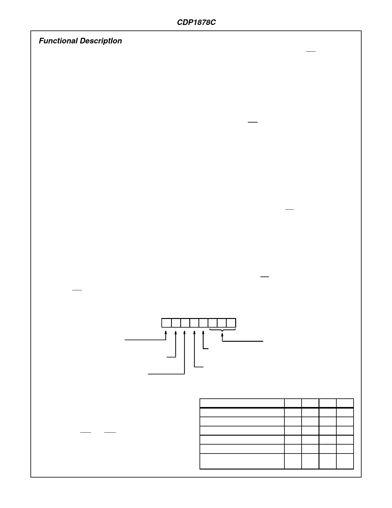
Control Register
76543210
JAM ENABLE
1 = ENABLE
0 = DISABLE
HOLDING REGISTER CONTROL
1 = FREEZE HOLDING REGISTER
0 = UPDATE CONTINUOUSLY
START/STOP CONTROL
1 = START COUNTER
0 = STOP COUNTER
GATE LEVEL SELECT
1 = POSITIVE (HIGH)
0 = NEGATIVE (LOW)
INTERRUPT ENABLE
1 = ENABLE
0 = DISABLE
MODE SELECT
001 = MODE 1
010 = MODE 2
†011 = MODE 3
100 = MODE 4
101 = MODE 5
†PLUS BIT 7 = 0
Bits 0, 1 and 2
Mode Selects - See Mode Timing Diagrams (Figures 1, 2, 3,
4, and 5).
Note: When selecting a mode, the timer outputs TAO and TBO
are set low, and TAO and TBO are set high. If bits 0, 1 and 2
are all zero’s when the control register is loaded, no mode is
selected, and the counter-timer outputs are unaffected. Issuing
mode 6 will cause an indeterminate condition of the counter,
issuing mode 7 is equivalent to issuing mode 5.
BIT 7 BIT 2 BIT 1 BIT 0
Mode 1 - Timeout
-
0
0
1
Mode 2 - Timeout Strobe
-
0
1
0
Mode 3 - Gate Controlled One Shot 0
0
1
1
Mode 4 - Rate Generator
-
1
0
0
Mode 5 - Variable-Duty Cycle
-
1
0
1
No Mode selected. Counter outputs -
0
0
0
unaffected
4-95
Share Link: 