TPC8127 View Datasheet(PDF) - Toshiba
Part Name
Description
Manufacturer
TPC8127 Datasheet PDF : 7 Pages
| |||
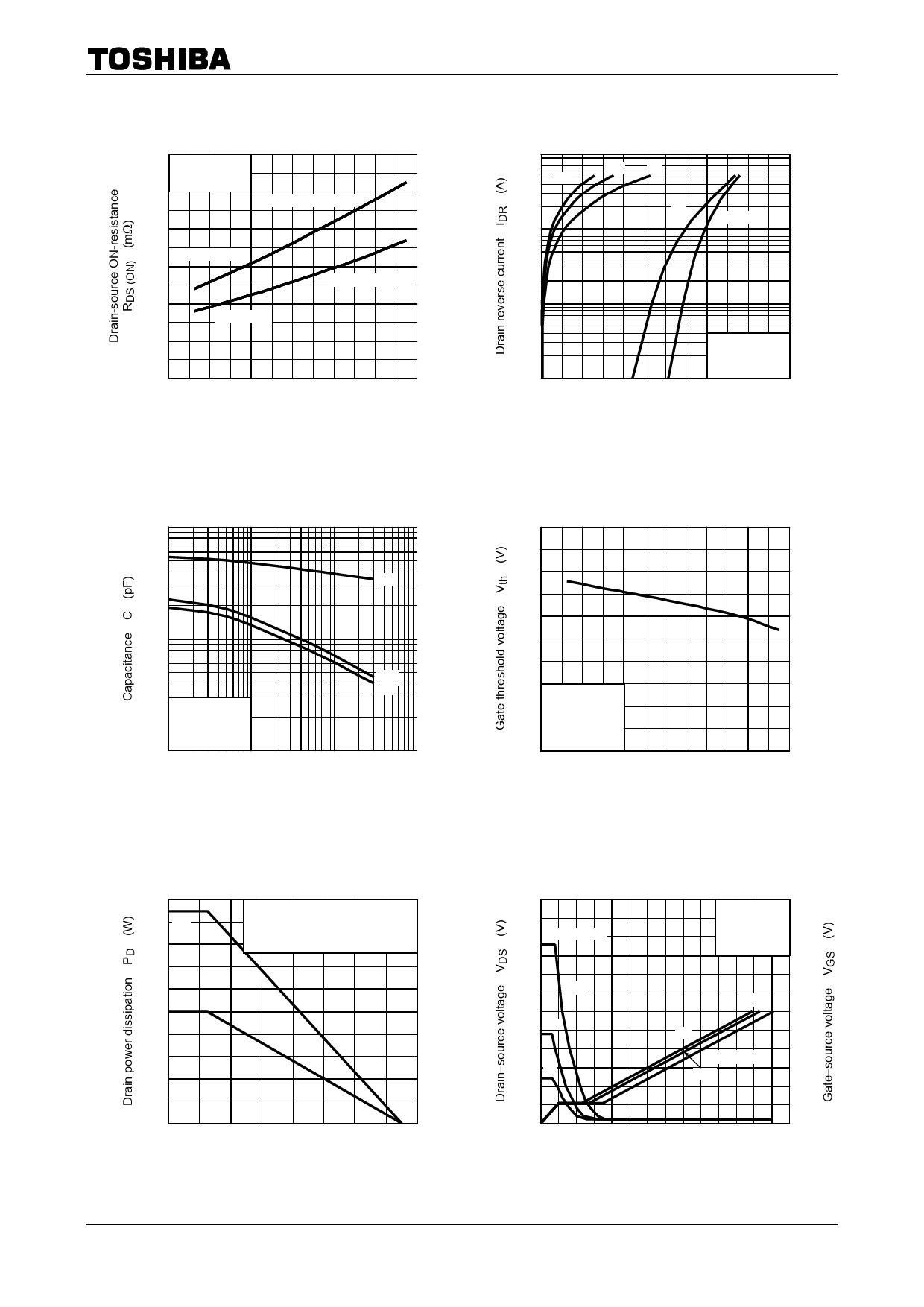
RDS (ON) – Ta
12
Common source
Pulse test
10
ID = −3, −6.5, −13 A
8
VGS = −4.5 V
6
4
VGS = −10 V
2
ID = −3, −6.5, −13 A
0
−80
−40
0
40
80
120
160
Ambient temperature Ta (°C)
TPC8127
−100
−10
−10
IDR – VDS
−4.5
−3
−1
VGS = 0 V
−1
−0.1
0
Common source
Ta = 25°C
Pulse test
0.2
0.4
0.6
0.8
1
1.2
Drain−source voltage VDS (V)
10000
Capacitance – VDS
Ciss
1000
Common source
VGS = 0 V
f = 1 MHz
Ta = 25°C
100
−0.1
−1
Coss
Crss
−10
−100
Drain−source voltage VDS (V)
Vth – Ta
−2
−1.6
−1.2
−0.8
Common source
−0.4 VDS = −10 V
ID = −0.5mA
Pulse test
0
−80
−40
0
40
80
120
160
Ambient temperature Ta (°C)
2
(1)
1.6
1.2
(2)
0.8
PD – Ta
(1)Device mounted on a glass-epoxy
board(a) (Note 2a)
(2)Device mounted on a glass-epoxy
board(b) (Note 2b)
t = 10 s
0.4
0
0
40
80
120
160
Ambient temperature Ta (°C)
Dynamic input/output
characteristics
−30
−25 VDD = −24 V
−30
Common source
ID = −13 A
Ta = 25°C
−25
Pulse test
−20
VDS
−15
−12
−10
−6
−5
−20
VGS
−15
−6
−10
VDD = −24 V
−12
−5
0
0
0
20
40
60
80
100 120 140
Total gate charge Qg (nC)
5
2009-11-20
Share Link: 