HB288256C5 View Datasheet(PDF) - Hitachi -> Renesas Electronics
Part Name
Description
Manufacturer
HB288256C5
Hitachi -> Renesas Electronics

HB288256C5 Datasheet PDF : 67 Pages
| |||
HB288256/192/160/128/096/064/032C5
2. Task File register access specifications
There are two cases of Task File register mapping, one is mapped I/O address area, the other is mapped Memory address
area. Each case of Task File register read and write operations are executed under the condition as follows. That area can
be accessed by Byte/Word/Odd Byte mode which are defined by PC card standard specifications.
(1) I/O address map
Task File Register Read Access Mode (1)
Mode
-REG -CE2 -CE1 A0
Standby mode
×
H
H
×
Byte access (8-bit)
L
H
L
L
L
H
L
H
Word access (16-bit) L
L
L
×
Odd byte access (8-bit) L
L
H
×
Note: ×: L or H
-IORD -IOWR -OE
×
×
×
L
H
H
L
H
H
L
H
H
L
H
H
-WE
×
H
H
H
H
D8 to D15 D0 to D7
High-Z High-Z
High-Z even byte
High-Z odd byte
odd byte even byte
odd byte High-Z
Task File Register Write Access Mode (1)
Mode
-REG -CE2 -CE1 A0
Standby mode
×
H
H
×
Byte access (8-bit)
L
H
L
L
L
H
L
H
Word access (16-bit) L
L
L
×
Odd byte access (8-bit) L
L
H
×
Note: ×: L or H
-IORD -IOWR -OE
×
×
×
H
L
H
H
L
H
H
L
H
H
L
H
-WE
×
H
H
H
H
D8 to D15 D0 to D7
Don’t care Don’t care
Don’t care even byte
Don’t care odd byte
odd byte even byte
odd byte Don’t care
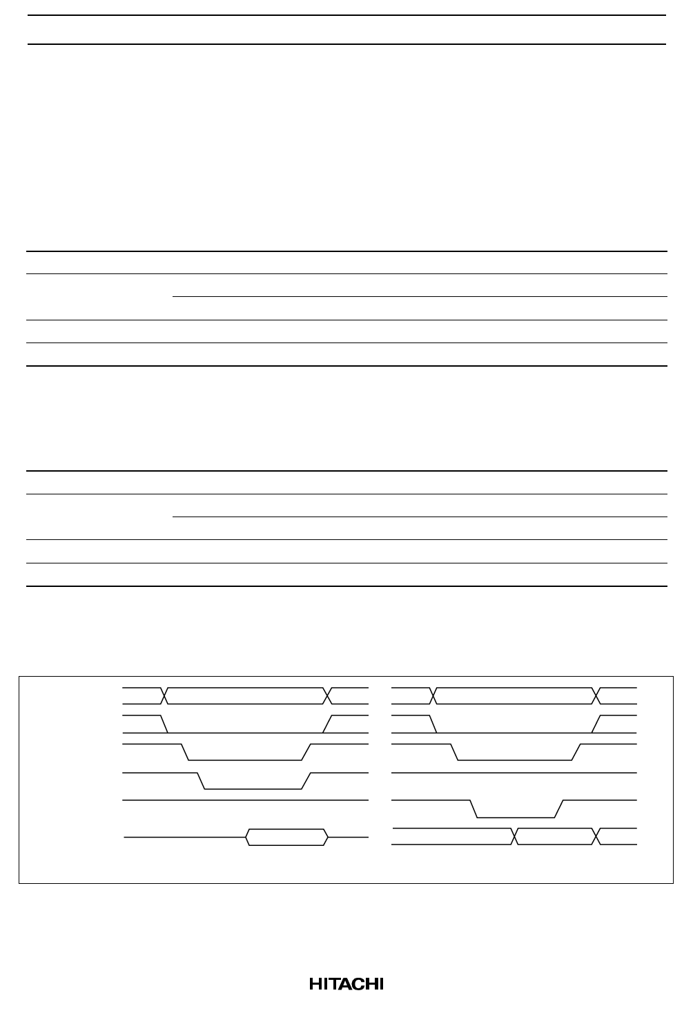
Task File Register Access Timing Example (1)
A0 to A10
-REG
-CE2/-CE1
-IORD
- IOWR
D0 to D15
Dout
read cycle
Din
write cycle
13
Share Link: