LTC1772HS6 View Datasheet(PDF) - Linear Technology
Part Name
Description
Manufacturer
LTC1772HS6 Datasheet PDF : 12 Pages
| |||
LTC1772
APPLICATIONS INFORMATION
0.4V, the loss increases from 0.5% to 8% as the load
current increases from 0.5A to 2A.
5. Transition losses apply to the external MOSFET and
increase at higher operating frequencies and input
voltages. Transition losses can be estimated from:
Transition Loss = 2(VIN)2IO(MAX)CRSS(f)
Other losses including CIN and COUT ESR dissipative
losses, and inductor core losses, generally account for
less than 2% total additional loss.
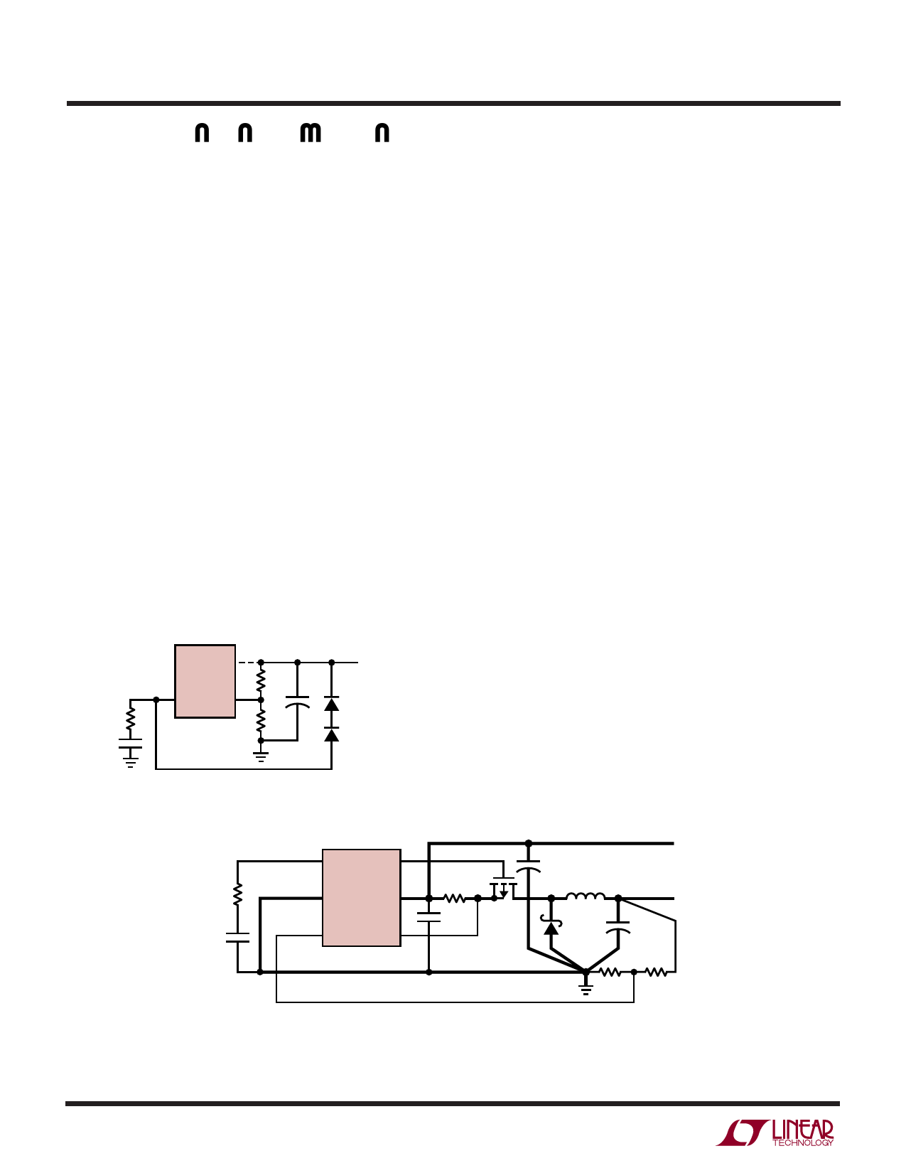
Foldback Current Limiting
As described in the Output Diode Selection, the worst-case
dissipation occurs with a short-circuited output when the
diode conducts the current limit value almost continu-
ously. To prevent excessive heating in the diode, foldback
current limiting can be added to reduce the current in
proportion to the severity of the fault.
Foldback current limiting is implemented by adding diodes
DFB1 and DFB2 between the output and the ITH/RUN pin as
shown in Figure 5. In a hard short (VOUT = 0V), the current
LTC1772
ITH/RUN VFB
R2 +
R1
VOUT
DFB1
DFB2
1772 F05
Figure 5. Foldback Current Limiting
will be reduced to approximately 50% of the maximum
output current.
PC Board Layout Checklist
When laying out the printed circuit board, the following
checklist should be used to ensure proper operation of the
LTC1772. These items are illustrated graphically in the
layout diagram in Figure 6. Check the following in your
layout:
1. Is the Schottky diode closely connected between ground
(Pin 2) and drain of the external MOSFET?
2. Does the (+) plate of CIN connect to the sense resistor
as closely as possible? This capacitor provides AC
current to the MOSFET.
3. Is the input decoupling capacitor (0.1µF) connected
closely between VIN (Pin 5) and ground (Pin 2)?
4. Connect the end of RSENSE as close to VIN (Pin 5) as
possible. The VIN pin is the SENSE + of the current
comparator.
5. Is the trace from SENSE– (Pin 4) to the Sense resistor
kept short? Does the trace connect close to RSENSE?
6. Keep the switching node PGATE away from sensitive
small signal nodes.
7. Does the VFB pin connect directly to the feedback
resistors? The resistive divider R1 and R2 must be
connected between the (+) plate of COUT and signal
ground.
RITH
CITH
1
6
ITH/RUN PGATE
LTC1772
2
5
GND
VIN
3
VFB
SENSE– 4
RSENSE
0.1µF
+
M1
CIN
L1
+
D1
COUT
VIN
VOUT
BOLD LINES INDICATE HIGH CURRENT PATHS
R1
R2
1772 F06
Figure 6. LTC1772 Layout Diagram (See PC Board Layout Checklist)
1772fb
10
Share Link: 