LTC1772HS6 View Datasheet(PDF) - Linear Technology
Part Name
Description
Manufacturer
LTC1772HS6 Datasheet PDF : 12 Pages
| |||
LTC1772
PIN FUNCTIONS
ITH/RUN (Pin 1): This pin performs two functions. It
serves as the error amplifier compensation point as well as
the run control input. The current comparator threshold
increases with this control voltage. Nominal voltage range
for this pin is 0.7V to 1.9V. Forcing this pin below 0.35V
causes the device to be shut down. In shutdown all
functions are disabled and the PGATE pin is held high.
GND (Pin 2): Ground Pin.
VFB (Pin 3): Receives the feedback voltage from an exter-
nal resistive divider across the output.
SENSE– (Pin 4): The Negative Input to the Current Com-
parator.
VIN (Pin 5): Supply Pin. Must be closely decoupled to GND
Pin 2.
PGATE (Pin 6): Gate Drive for the External P-Channel
MOSFET. This pin swings from 0V to VIN.
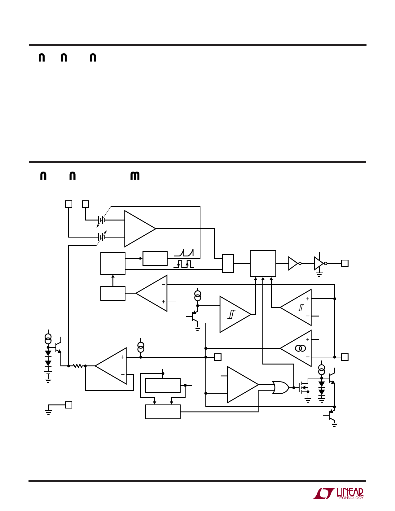
W
FUNCTIONAL DIAGRA
VIN SENSE–
5
4
+
ICMP
–
SLOPE
OSC
COMP
RS1
R
Q
S
SWITCHING
LOGIC AND
BLANKING
CIRCUIT
VIN
PGATE
6
VIN
0.3V
GND
2
FREQ
FOLDBACK
SHORT-CIRCUIT
DETECT
0.3V
0.15V
BURST
+
CMP
–
SLEEP
0.5µA
VIN
VOLTAGE
REFERENCE
UNDERVOLTAGE
LOCKOUT
1 ITH/RUN
0.35V
VREF
0.8V
+
SHDN
CMP
–
SHDN
UV
OVP
EAMP
VREF
+
60mV
VREF
0.8V
VFB
3
VIN
1.2V
1772 FD
1772fb
4
Share Link: 