LTC1772HS6 View Datasheet(PDF) - Linear Technology
Part Name
Description
Manufacturer
LTC1772HS6 Datasheet PDF : 12 Pages
| |||
LTC1772
APPLICATIONS INFORMATION
Low Supply Operation
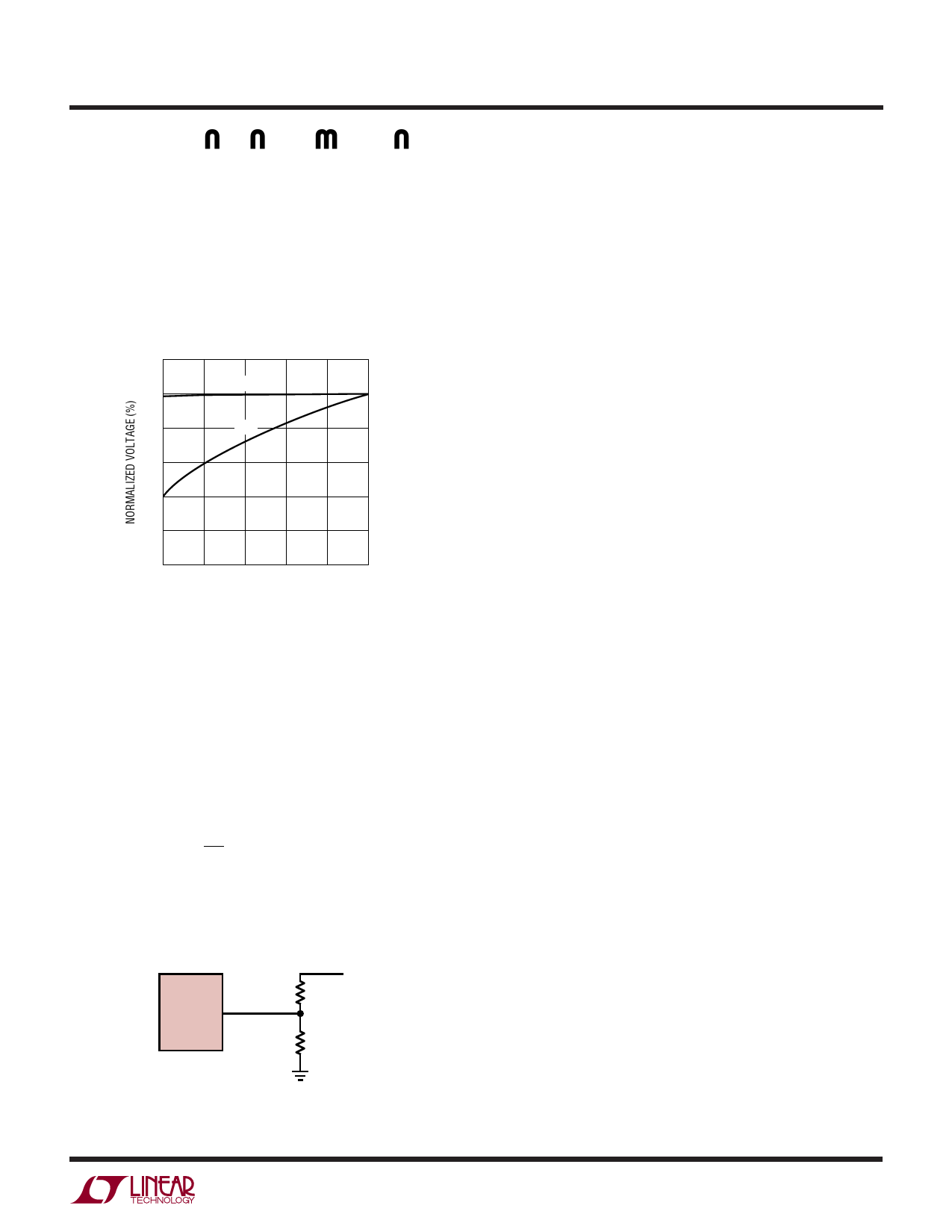
Although the LTC1772 can function down to approxi-
mately 2V, the maximum allowable output current is
reduced when VIN decreases below 3V. Figure 3 shows the
amount of change as the supply is reduced down to 2V.
Also shown in Figure 3 is the effect of VIN on VREF as VIN
goes below 2.3V.
105
VREF
100
95
VITH
90
85
80
75
2.0
2.2
2.4
2.6
2.8
3.0
INPUT VOLTAGE (V)
1772 F03
Figure 3. Line Regulation of VREF and VITH
Setting Output Voltage
The LTC1772 develops a 0.8V reference voltage between
the feedback (Pin 3) terminal and ground (see Figure 4). By
selecting resistor R1, a constant current is caused to flow
through R1 and R2 to set the overall output voltage. The
regulated output voltage is determined by:
VOUT = 0.8⎛⎝⎜1+ RR21⎞⎠⎟
For most applications, an 80k resistor is suggested for R1.
To prevent stray pickup, locate resistors R1 and R2 close
to LTC1772.
LTC1772
3
VFB
VOUT
R2
R1
1772 F04
Figure 4. Setting Output Voltage
Efficiency Considerations
The efficiency of a switching regulator is equal to the
output power divided by the input power times 100%. It is
often useful to analyze individual losses to determine what
is limiting the efficiency and which change would produce
the most improvement. Efficiency can be expressed as:
Efficiency = 100% – (η1 + η2 + η3 + ...)
where η1, η2, etc. are the individual losses as a percent-
age of input power.
Although all dissipative elements in the circuit produce
losses, four main sources usually account for most of the
losses in LTC1772 circuits: 1) LTC1772 DC bias current,
2) MOSFET gate charge current, 3) I2R losses and 4)
voltage drop of the output diode.
1. The VIN current is the DC supply current, given in the
electrical characteristics, that excludes MOSFET driver
and control currents. VIN current results in a small loss
which increases with VIN.
2. MOSFET gate charge current results from switching
the gate capacitance of the power MOSFET. Each time
a MOSFET gate is switched from low to high to low
again, a packet of charge dQ moves from VIN to ground.
The resulting dQ/dt is a current out of VIN which is
typically much larger than the DC supply current. In
continuous mode, IGATECHG = f(Qp).
3. I2R losses are predicted from the DC resistances of the
MOSFET, inductor and current shunt. In continuous
mode the average output current flows through L but
is “chopped” between the P-channel MOSFET (in se-
ries with RSENSE) and the output diode. The MOSFET
RDS(ON) plus RSENSE multiplied by duty cycle can be
summed with the resistances of L and RSENSE to obtain
I2R losses.
4. The output diode is a major source of power loss at
high currents and gets worse at high input voltages.
The diode loss is calculated by multiplying the forward
voltage times the diode duty cycle multiplied by the
load current. For example, assuming a duty cycle of
50% with a Schottky diode forward voltage drop of
1772fb
9
Share Link: 