FAN5250 View Datasheet(PDF) - Fairchild Semiconductor
Part Name
Description
Manufacturer
FAN5250 Datasheet PDF : 17 Pages
| |||
FAN5250
Output Voltage Programming
The output voltage of the converter is programmed by an
internal DAC in discrete steps between 0.6V and 1.75V:
Table 1. Output Voltage VID
VID4
1
1
1
1
1
1
1
1
1
1
1
1
1
1
1
1
0
0
0
0
0
0
0
0
0
0
0
0
0
0
0
0
VID3
1
1
1
1
1
1
1
1
0
0
0
0
0
0
0
0
1
1
1
1
1
1
1
1
0
0
0
0
0
0
0
0
VID2
1
1
1
1
0
0
0
0
1
1
1
1
0
0
0
0
1
1
1
1
0
0
0
0
1
1
1
1
0
0
0
0
VID1
1
1
0
0
1
1
0
0
1
1
0
0
1
1
0
0
1
1
0
0
1
1
0
0
1
1
0
0
1
1
0
0
1 = Logic High or open, 0 = Logic Low
VID0
1
0
1
0
1
0
1
0
1
0
1
0
1
0
1
0
1
0
1
0
1
0
1
0
1
0
1
0
1
0
1
0
VOUT to
CPU
0.600
0.625
0.650
0.675
0.700
0.725
0.750
0.775
0.800
0.825
0.850
0.875
0.900
0.925
0.950
0.975
1.000
1.050
1.100
1.150
1.200
1.250
1.300
1.350
1.400
1.450
1.500
1.550
1.600
1.650
1.700
1.750
VID0–4 pins will assume a logic 1 level if left open as each
has a 12µA internal current source pull-up to 2.5V. The
output of the DAC voltage also establishes the thresholds for
PGOOD, UVP and OVP thresholds.
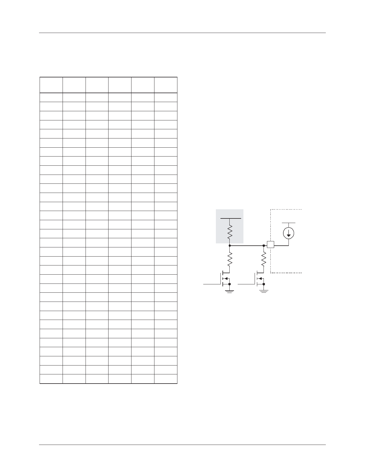
Alternative Voltage Programming Input
The output voltage can alternatively be set by the ALTV pin.
This override of the VID DAC becomes necessary during
power-up and some power saving modes of operation, when
the voltage on the processor is insufficient to provide correct
VID codes to the controller. Therefore, the required core
voltage should be set by some means external to the
processor. A common approach to this problem is to provide
hard-wired VID codes via a multiplexer controlled by the
CPU. That approach lacks simplicity and takes many
external components and valuable motherboard area.
The FAN5250 uses a simpler way to set the core voltages
when the CPU is incapable of providing valid VID codes.
A resistor-MOSFET network (shown in Figure 4) works
with the calibrated 10µA current from the ALTV pin to set
the ALTV voltage when the MOSFET's gate is driven high.
The controller regulates the output voltage to the level
established on the ALTV pin when this voltage is lower than
the highest VID programmed voltage (1.75V). When both
MOSFET gates are low, the ALTV pin goes to 2.5V and the
output is controlled by the VID code. If a more accurate
Deep-Sleep (DSX) and Start voltages are required than the
internal current source can provide, it may be overridden
with the external resistor shown (grey-shading).
REF
Rx
ALTV 6
2.5V
10?A
R7
R8
START
DSX
Figure 4. ALTV Programming
When relying on the internal current source to set ALTV:
R7
=
V----1-S--0-T---µA---A-R----T-
and⋅
R8
=
1-V---0-D---µ-S--A-X--
(4)
When using Rx for greater accuracy, on the internal current
source to set ALTV, Choose a value for Rx where
V-----R---E----F----–-R----V-X---S----T---A---R----T-
»
10 µ A ,
then
R7
=
V-----R---E----F----–-----V----S-V--T---×-A---R-V---T-S---+-T---A-(--R-R---T-X-----×-----1---0----µ---A-----)
(5)
R8
=
-V----R---E----F----–-----V-R---D---×-S---X-V----+S----T-(--AR---R--X--T--×-----1----0---µ----A-----)
8
REV. 1.1.6 3/12/03
Share Link: 