UPD16434G-001-12 View Datasheet(PDF) - NEC => Renesas Technology
Part Name
Description
Manufacturer
UPD16434G-001-12 Datasheet PDF : 64 Pages
| |||
µ PD16434
2. INTERNAL BLOCK FUNCTIONS
2.1 Serial/Parallel Interface
The µ PD16434 contains both serial and parallel interface functions. Whether the serial interface or the parallel
interface is used is determined by whether the P, /S input is high (specifying the parallel interface) or low
(specifying the serial interface) at the RESET signal falling edge.
The interface circuit is used to write commands and data from the CPU or output data to the CPU.
The operation of the serial/parallel interface differs, depending on the data processing mode setting. When a
RESET is input, the data processing mode is initialized to the write mode, so that the first command input can be
accepted. Afterwards, the mode can be set to write related or read related data processing mode by the data
processing set command.
If the data processing mode is set to the write, AND, OR, or the character write related mode, the serial/parallel
interface is set to the data input mode, and the µ PD16434 clocks in the data from the SI pin (serial data) or from the D3
to D0 pins (4-bit parallel data) in synchronization with the rising edge of the /SCK or the /STB, respectively.
If the data processing mode is set to the read mode, the serial/parallel interface becomes the data output mode
and outputs data from the SO pin (serial data) or from the D3 to D0 pins (4-bit parallel data) in synchronization with the
falling edge of the /SCK or the /STB.
The serial/parallel register serves as the buffer, between 8-bit serial data or two 4-bit parallel data transferred
through the serial input/output (SI, SO) or parallel input/output (D3 to D0) and 8-bit parallel data of the data memory.
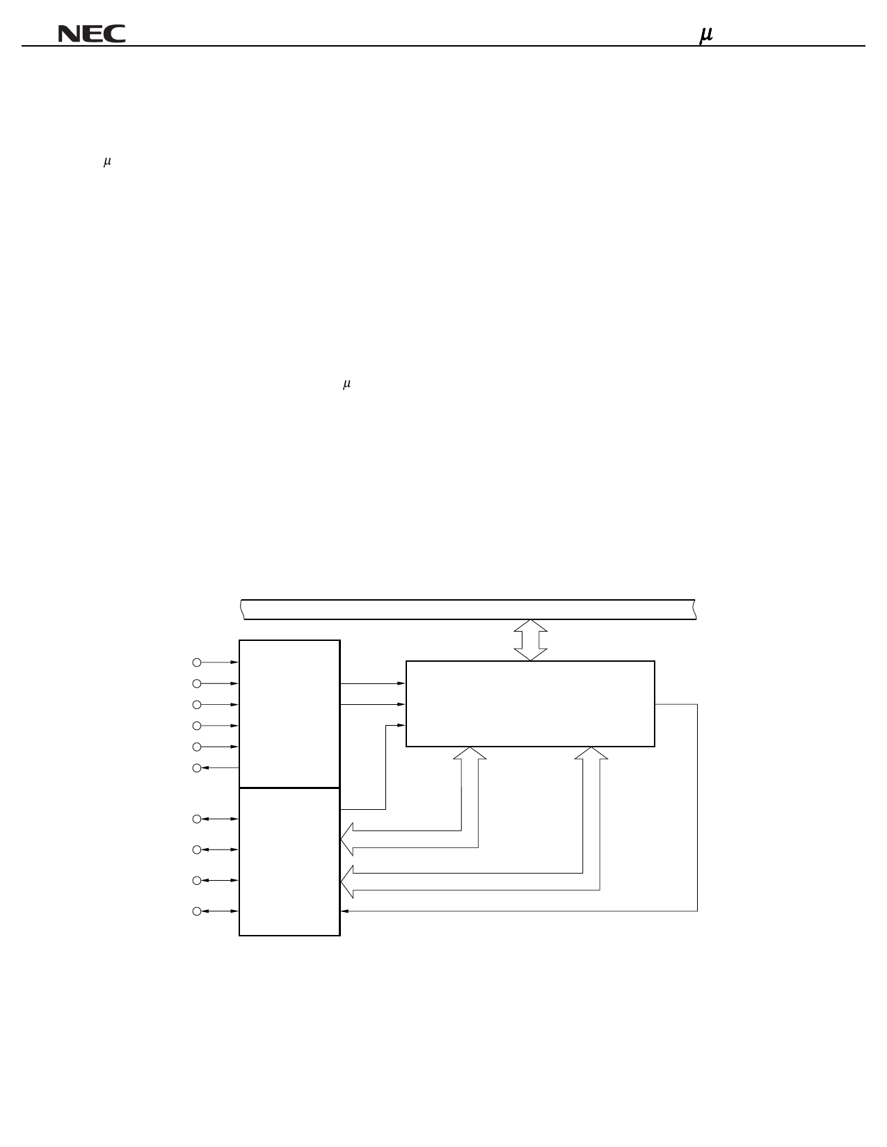
Figure 2–1. Serial/Parallel Interface
/STB, /SCK
RESET
/CS
CA0,CA1
C, /D
/BUSY
Internal bus
8
/STB'
Read/write
/SCK'
8-bit serial/parallel register
SO'
control
SI'
bit 0-3
bit 4-7
4
4
D0/SI
D1(P, /S)
D2(CAE)
D3/SO
Data
control
10
Data Sheet S10299EJ4V0DS00
Share Link: 