UPD16640CN View Datasheet(PDF) - NEC => Renesas Technology
Part Name
Description
Manufacturer
UPD16640CN Datasheet PDF : 16 Pages
| |||
µ PD16640C
5. RELATIONSHIP BETWEEN INPUT DATA AND OUTPUT PIN
Data format : 6 bits x RGB(3 dots)
Input width : 18 bits
(1) R,/L = H (right shift)
Output
S1
S2
S3
…
S308
S309
Data
D00 to D05 D10 to D15 D20 to D25
…
D10 to D15 D20 to D25
(2) R,/L = L (left shift)
Output
S1
S2
S3
…
S299
S300
Data
D00 to D05 D10 to D15 D20 to D25
…
D10 to D15 D20 to D25
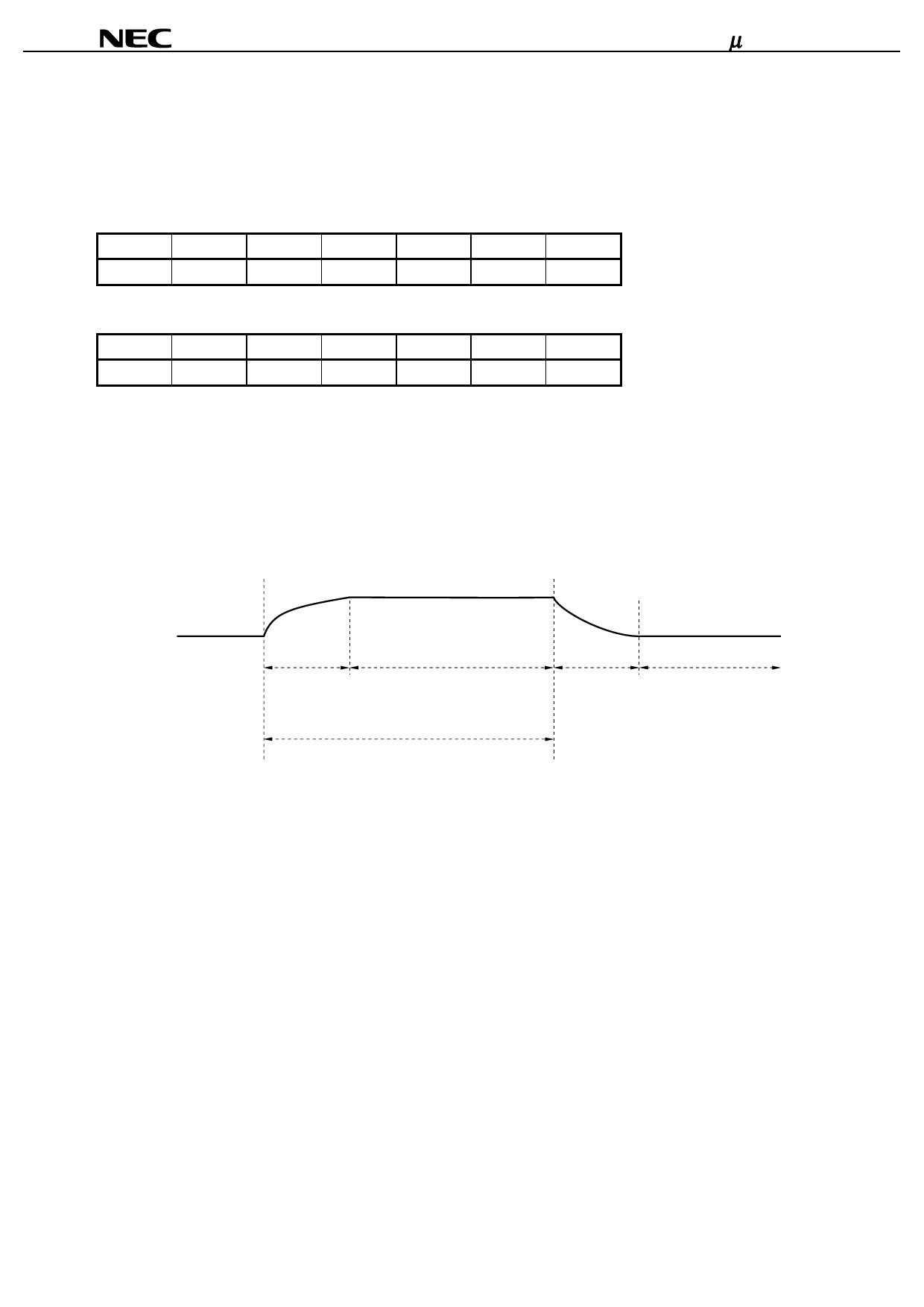
6. OPERATION OF OUTPUT BUFFER
The output buffer consists of an operational amplifier circuit that does not perform precharge operation.
Therefore, driver output current IVOH1/2 is the charging current to the LCD, and IVOL1/2 is the discharging current.
Figure 6-1. LCD Panel Driving Waveform
VDD2
Sn
VSS2
Write
(IVOL1/2/IVOH1/2)
1 horizontal period
Write
(IVOL1/2/IVOH1/2)
8
Data Sheet S11269EJ1V1DS00
Share Link: 