UPD16704P View Datasheet(PDF) - NEC => Renesas Technology
Part Name
Description
Manufacturer
UPD16704P Datasheet PDF : 14 Pages
| |||
µ PD16704
Pin Symbol
Pin Name
VSS
Logic ground
VEE1
Negative power
supply for internal
operation
VEE2
Driver negative
power supply
Pad No
30 - 33
7 - 10,
39 - 42
3 - 6,
43 - 46
I/O
Description
– Connect this pin to the ground of the system.
– –15 to –5 V
– The driver output: low level (VEE2 to VEE1 < 6.0 V)
(2/2)
Cautions 1. To prevent latch-up, turn on power to VDD1, VEE1, VEE2, VDD2, and logic input in this order. Turn off
power in the reverse order. These power up/down sequence must be observed also during
transition period.
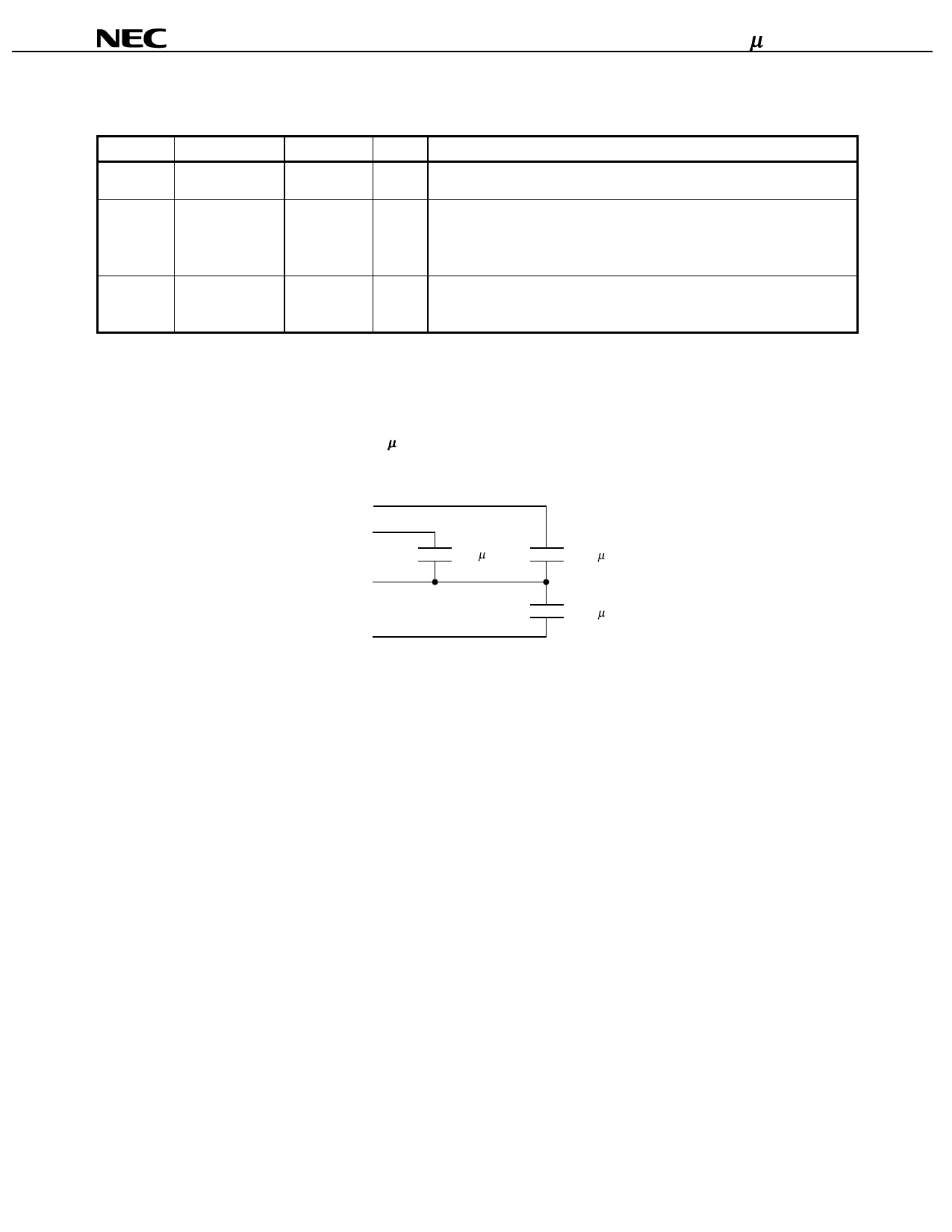
2. Insert a capacitor of about 0.1 µF between each power line, as shown below, to secure noise margin
such as VIH and VIL.
VDD2
VDD1
VSS
VEE1
VEE2
0.1 µ F
0.1 µF
0.1 µF
8
Data Sheet S15809EJ1V0DS
Share Link: 