UPD17236MC View Datasheet(PDF) - NEC => Renesas Technology
Part Name
Description
Manufacturer
UPD17236MC
NEC => Renesas Technology

UPD17236MC Datasheet PDF : 92 Pages
| |||
µPD17230, 17231, 17232, 17233, 17234, 17235, 17236
APPLICATION
Preset remote controllers, toys, portable systems, etc.
ORDERING INFORMATION
Part Number
µPD17230MC-×××-5A4
µPD17231MC-×××-5A4
µPD17232MC-×××-5A4
µPD17233MC-×××-5A4
µPD17234MC-×××-5A4
µPD17235GT-×××
µPD17235MC-×××-5A4
µPD17236GT-×××
µPD17236MC-×××-5A4
Package
30-pin plastic shrink SOP (300 mil)
30-pin plastic shrink SOP (300 mil)
30-pin plastic shrink SOP (300 mil)
30-pin plastic shrink SOP (300 mil)
30-pin plastic shrink SOP (300 mil)
28-pin plastic SOP (375 mil)
30-pin plastic shrink SOP (300 mil)
28-pin plastic SOP (375 mil)
30-pin plastic shrink SOP (300 mil)
Remark ××× indicates ROM code suffix.
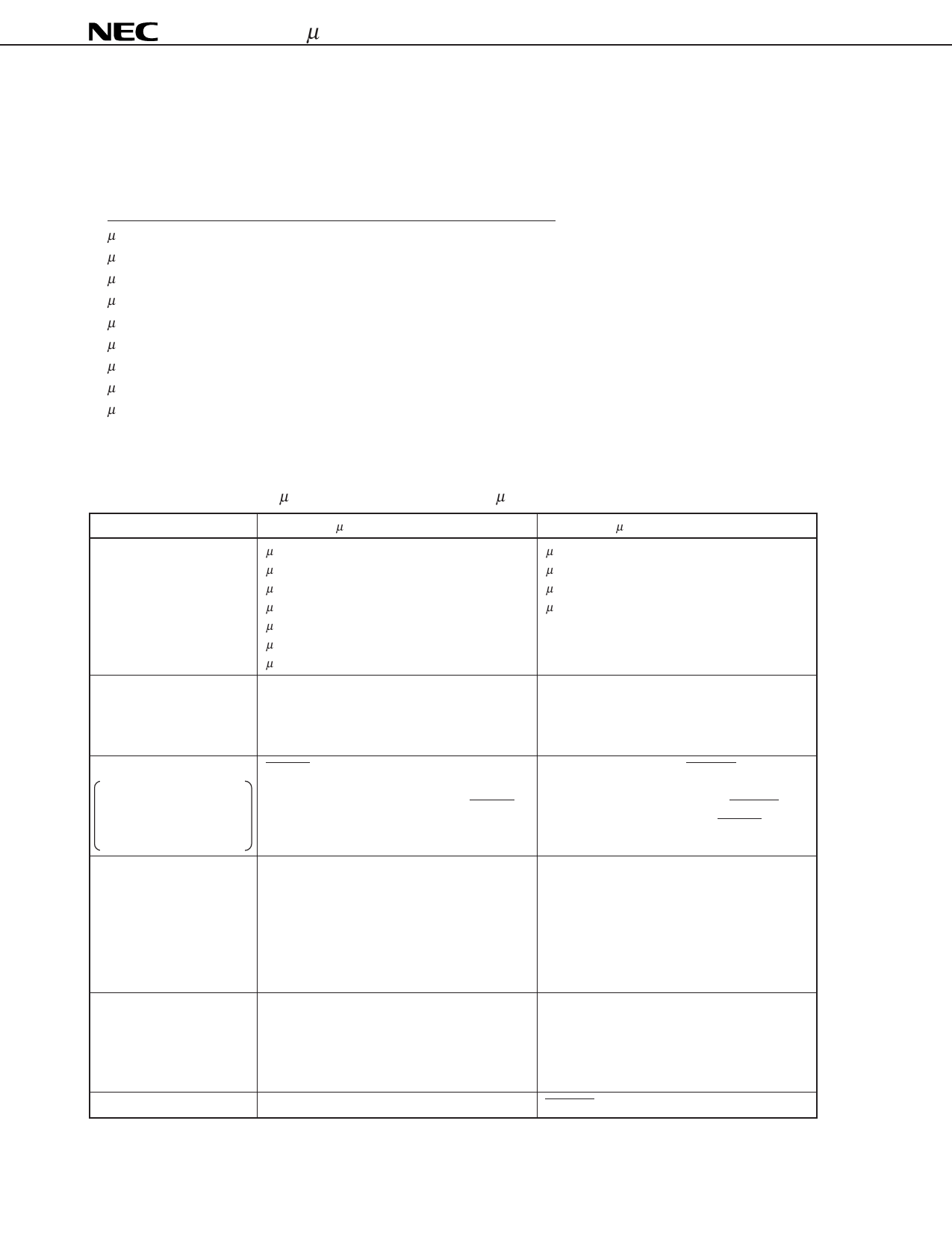
DIFFERENCE BETWEEN µPD17236 SUBSERIES AND µPD17225 SUBSERIES
Item
ROM capacity
Port
Reset
• Reset by watchdog timer
• Reset by stack pointer
• Low-voltage detection
circuit (mask option)
STOP mode release
condition
Carrier frequency
(fX = 4 MHz)
Pin 14
µPD17236 Subseries
µPD17225 Subseries
µPD17230: 2048 × 16 bits
µPD17231: 4096 × 16 bits
µPD17232: 6144 × 16 bits
µPD17233: 8192 × 16 bits
µPD17234: 10240 × 16 bits
µPD17235: 12288 × 16 bits
µPD17236: 16384 × 16 bits
µPD17225: 2048 × 16 bits
µPD17226: 4096 × 16 bits
µPD17227: 6144 × 16 bits
µPD17228: 8192 × 16 bits
P0B0-P0B3: I/O (bit I/O)
P0C0-P0C3: I/O (group I/O)
P0D0-P0D3: I/O (group I/O)
P1A0: Input or output selectable by mask option
P0B0-P0B3: Input
P0C0-P0C3: Output
P0D0-P0D3: Output
RESET pin is internally pulled down by
occurrence of the internal reset signals on the
left, and reset takes place (usually, RESET pin
is pulled up).
Low level is output from WDOUT pin by
occurrence of the internal reset signals on the
left, and reset takes place if the WDOUT pin
is externally connected to the RESET pin.
<1> When any of pins P0A0-P0A3 goes low
<2> When P0B0-P0B3, P0C0-P0C3, and
P0D0-P0D3 are used as input pins and
any of them goes low
<3> When the interrupt request (IRQ) of an
interrupt for which IP flag is set is
generated at rising or falling edge of INT pin
When any of P0A0-P0A3 or P0B0-P0B3 goes
low
Selected by mask option
<1> If carrier generation clock (RfX) is fX/2:
7.8 kHz to 1 MHz
<2> If carrier generation clock (RfX) is fX:
15.6 kHz to 2 MHz
7.8 kHz to 1 MHz
P1A0 pin
WDOUT pin
2
Data Sheet U14360EJ1V0DS00
Share Link: