UPD4712D View Datasheet(PDF) - NEC => Renesas Technology
Part Name
Description
Manufacturer
UPD4712D Datasheet PDF : 12 Pages
| |||
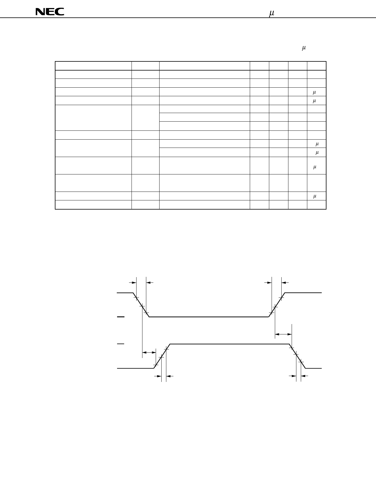
µPD4712C/4712D
ELECTRICAL CHARACTERISTICS (DRIVER)
(Unless otherwise specified, VCC = +5 V ±10 %, TA = –20 ˚C to +80 ˚C, C1 to C4 = 22 µF)
Parameter
Low-level input voltage
High-level input voltage
Low-level input current
High-level input current
Output voltage
Output short current
Slew rate
Propagation delay time Note 4
Output resistance
Standby output transition time
Standby output transition time
Symbol
VIL
VIH
IIL
IIH
VDO
ISC
SR
tPHL
tPLH
RO
tDAZ
tDZA
Conditions
VCC = +5.0 V, RL = ∞, TA = 25 ˚C
VCC = +5.0 V, RL = 3 kΩ
VCC = +4.5 V, RL = 3 kΩ
VCC = +5.0 V, vs. GND
CL = 10 pF, RL = 3 to 7 kΩ
CL = 2500 pF, RL = 3 to 7 kΩ
RL = 3.5 kΩ, CL = 2500 pF
VCC = VDD = VSS = 0 V
VOUT = ±2 V
Note 5
Note 5
MIN.
2.0
0
0
±5.5
±5.0
1.5
1.5
TYP.
±9.7
±15
9
5
MAX.
0.8
–1.0
1.0
±40
30
30
Unit
V
V
µA
µA
V
V
V
mA
V/µs
V/µs
0.8
µs
300
4
25
Ω
10 µs
50 ms
* TYP.: Typical (reference) value at TA = 25 ˚C.
Note 4. Test point
If the output control pin is made low, the driver output goes low regardless of the driver input state.
6 ns
6 ns
Driver input
5
90 %
1.5 V
0
10 %
VOH
Driver output
VOL
tPLH
10 %
3V
–3 V
SR
10 %
90 %
1.5 V
tPHL
3V
–3 V
90 %
SR
5
Share Link: 