UPD6125A View Datasheet(PDF) - NEC => Renesas Technology
Part Name
Description
Manufacturer
UPD6125A Datasheet PDF : 40 Pages
| |||
µPD6125A, 6126A
11.3 I/O Pin (P3, P4 ) Note
P3/P4 are input/output pins for adding a key matrix. The LSB of control registers P13 and P14 switches between
input and output modes.
When in input mode, all pins are pulled down by the LSI to the VSS level.
When “all clear” is input or on reset, input mode goes into effect, and the output latch value becomes undefined.
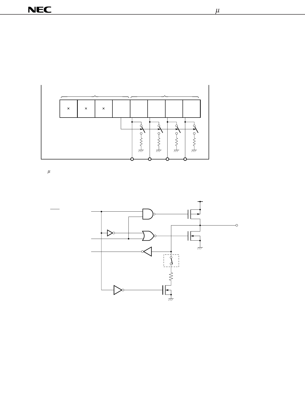
Figure 11-2. I/O Pin Organization
P3/P4
Note
P13, P14
Note
P03, P04
IN/OUT I/O3
I/O2
I/O1
I/O0
IN/OUT
0 ······· Input mode
1 ······· Output mode
P3 ··· I/O00 to I/O03,
P4 ··· I/O10 to I/O13
Note µPD6125A is not equipped with P13, P14, P03, and P04.
11.4 I/O Pull-Down Resistor Organization
Input/output selection
Output signal
Input signal
VDD
P-ch
Pin
N-ch
CMOS
VSS
I/O pull-down resistor switch
(Mask option)
R Pull-down resistor
Nch
The use of pull-down resistors for I/O can be selected by using the mask option.
When the pull-down resistor switch is turned on (1 is set) by the mask option, the pull-down resistor R is turned
on only in input mode.
Caution When using the pins as key switches, turn on the pull-down resistor switch by the mask option.
10
Share Link: 