UPD6134GS-XXX-E1 View Datasheet(PDF) - NEC => Renesas Technology
Part Name
Description
Manufacturer
UPD6134GS-XXX-E1
NEC => Renesas Technology

UPD6134GS-XXX-E1 Datasheet PDF : 64 Pages
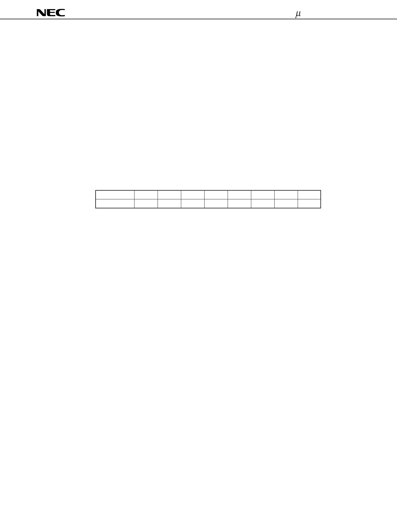
| |||
µPD6133, 6134
3.1 KI/O Port (P0)
The KI/O port is an 8-bit input/output port for key scan output.
INPUT/OUTPUT mode is set by bit 1 of the P4 register.
If a read instruction is executed, the pin state can be read in INPUT mode, whereas the output latch contents
can be read in OUTPUT mode.
If the write instruction is executed, data can be written to the output latch regardless of INPUT or OUTPUT mode.
When reset, the port is placed in OUTPUT mode; and the value of the output latch (P0) becomes 1111 1111B.
The KI/O port contains the pull-down resistor, allowing pull-down in INPUT mode only.
Caution During double pressing of a key, a high-level output and a low-level output may coincide with
each other at the KI/O port. To avoid this, the low-level output current of the KI/O port is held
low. Therefore, be careful when using the KI/O port for purposes other than key scan output.
The KI/O port is so designed that, even when connected directly to VDD within the normal supply
voltage range (VDD = 1.8 to 3.6 V), no problem may occur.
Bit
Name
Table 3-2. KI/O Port (P0)
b7
KI/O7
b6
KI/O6
b5
KI/O5
b4
KI/O4
b3
KI/O3
b2
KI/O2
b1
KI/O1
b0
KI/O0
b0-b7
: In reading : In INPUT mode, the KI/O pin’s state is read.
In OUTPUT mode, the KI/O pin’s output latch contents are read.
In writing : Data is written to the KI/O pin’s output latch regardless of INPUT or OUTPUT mode.
Data Sheet U10454EJ6V0DS00
15
Share Link: