UPD754302GSA-XXX View Datasheet(PDF) - NEC => Renesas Technology
Part Name
Description
Manufacturer
UPD754302GSA-XXX Datasheet PDF : 74 Pages
| |||
µPD754302, 754304, 754302(A), 754304(A)
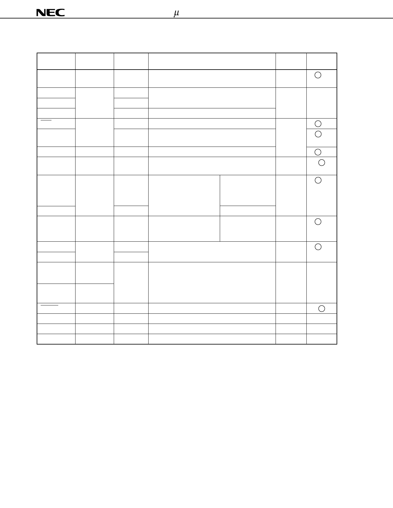
3.2 Non-port Pins
Pin Name
TI0/TI1
PTO0
PTO1
PCL
SCK
SO/SB0
SI
INT4
INT0
INT1
INT2
KR0-KR3
KR4-KR7
X1
X2
RESET
IC
VDD
VSS
Input/Output
Input
Output
Input/Output
Input
Input
Input
Input
Input
Input
–
Input
–
–
–
Alternate
Function
P13
P20
P21
P22
P01
P02
P03
P00
P10
P11
P12
P60-P63
P70-P73
–
–
–
–
–
Function
Inputs external event pulses to the timer/event
counter.
Timer/event counter output
I/O Circuit
After Reset TYPE Note
Input
B -C
Input
E-B
Clock output
Serial clock input/output
Serial data output
Serial data bus input/output
Serial data input
Edge detection vectored interrupt input (both
rising edge and falling edge detection)
Edge detection vectored
interrupt input (detection
edge can be selected).
INT0/P10 can select a
noise elimination circuit.
Asynchronous with
noise elimination
circuit can be selected
Asynchronous
Edge detection testable
input
(rising edge detection)
Asynchronous
Testable input (falling edge detection)
Input
Input
Input
Input
Input
F -A
F -B
B -C
B
B -C
B -C
F -A
Crystal/ceramic connection pin for the system
–
–
clock oscillator. When inputting the external
clock, input the external clock to pin X1, and
the inverted phase of the external clock to
pin X2.
System reset input (low-level active)
–
B
Internally connected. Connect directly to VDD.
–
–
Positive power supply
–
–
Ground potential
–
–
Note Circled characters indicate the Schmitt-trigger input.
10
Share Link: 