UPD75P0076GT View Datasheet(PDF) - NEC => Renesas Technology
Part Name
Description
Manufacturer
UPD75P0076GT Datasheet PDF : 62 Pages
| |||
µPD75P0076
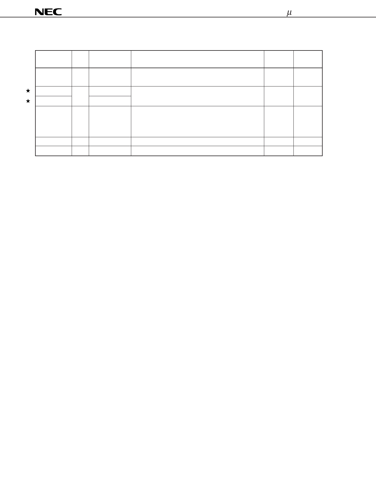
3.2 Non-port Pins (2/2)
Pin name I/O Alternate function
Function
After
reset
MD0 to MD3 I P30 to 33
Mode selection for program memory (PROM)
write/verify.
Input
D0 to D3
I/O P40 to 43
Data bus pin for program memory (PROM) write/verify. Input
D4 to D7
P50 to 53
VPPNote
—
—
Programmable voltage supply in program memory
—
(PROM) write/verify mode.
In normal operation mode, connect directly to VDD.
Apply +12.5 V in PROM write/verify mode.
VDD
—
—
Positive power supply
—
VSS
—
—
Ground
—
Note During normal operation, the VPP pin will not operate normally unless connected to VDD pin.
Circuit
type
E-B
M-E
—
—
—
8
Share Link: 