UPD75P3018AGC-8BT View Datasheet(PDF) - NEC => Renesas Technology
Part Name
Description
Manufacturer
UPD75P3018AGC-8BT Datasheet PDF : 64 Pages
| |||
µPD75P3018A
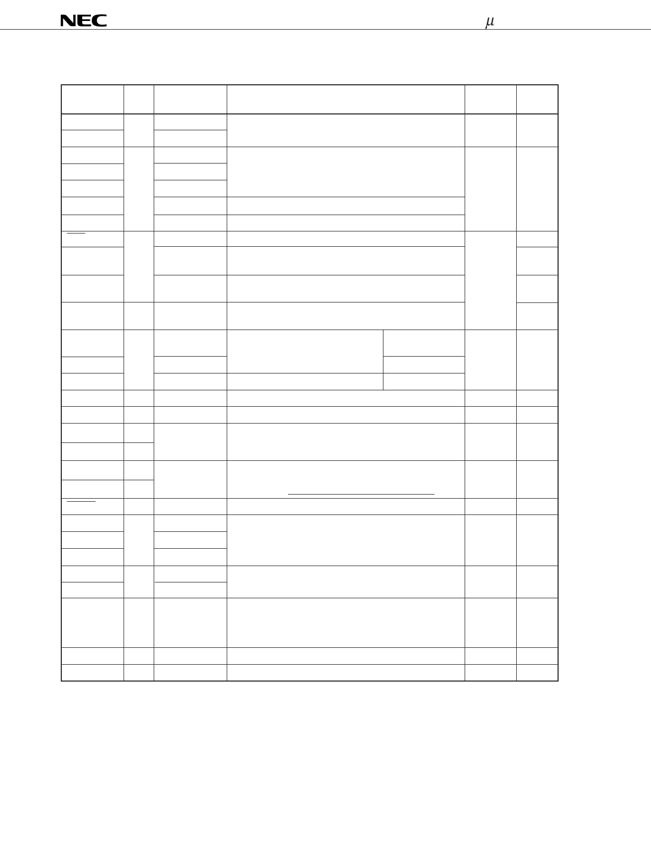
3.2 Non-port Pins (1/2)
Pin Name
TI0
TI1, TI2
PTO0
PTO1
PTO2
PCL
BUZ
SCK
SO/SB0
SI/SB1
INT4
INT0
INT1
INT2
KR0-KR3
KR4-KR7
X1
X2
XT1
XT2
RESET
MD0
MD1
MD2, MD3
D0-D3
D4-D7
VPPNote 2
VDD
Vss
I/O Alternate Function
Function
After Reset I/O Circuit
TypeNote 1
Input P13
External event pulse input to timer/event counter
Input
<B>-C
P12/INT2
Output P20
Timer/event counter output
Input
E-B
P21
P22
P22
Clock output
P23
Optional frequency output (for buzzer or system clock trimming)
I/O P01
Serial clock I/O
Input
<F>-A
P02
Serial data output
Serial data bus I/O
<F>-B
P03
Serial data input
Serial data bus I/O
<M>-C
Input P00
Edge detection vectored interrupt input
<B>
(both rising and falling edges detection)
Input P10
Edge detection vectored interrupt input Noise elimination circuit/
(detected edge is selectable)
asynchronous is selectable
Input
<B>-C
P11
INT0/P10 can select noise elimination circuit. Asynchronous
P12/TI1/TI2
Rising edge detection testable input Asynchronous
Input P60-P63
Falling edge detection testable input
Input
<F>-A
Input P70-P73
Falling edge detection testable input
Input
<F>-A
Input
—
Ceramic/crystal oscillation circuit connection for main system
—
—
clock. If using an external clock, input to X1 and input
—
inverted phase to X2.
Input
—
Crystal oscillation circuit connection for subsystem clock.
—
—
If using an external clock, input to XT1 and input inverted
—
phase to XT2. XT1 can be used as a 1-bit (test) input.
Input
—
System reset input (low level active)
—
<B>
Input P30/LCDCL
Mode selection for program memory (PROM) write/verify
Input
E-B
P31/SYNC
P32, P33
I/O P40-P43
Data bus for program memory (PROM) write/verify
Input
M-E
P50-P53
—
—
Program power supply voltage for program memory
(PROM) write/verify.
For normal operation, connect directly to VDD.
Apply +12.5 V for PROM write/verify.
—
—
—
—
Positive power supply
—
—
—
—
Ground
—
—
Notes 1. Circuit types enclosed in brackets indicate Schmitt trigger input.
2. The VPP pin does not operate correctly during normal operation unless connected to the VDD pin.
8
Data Sheet U11917EJ2V0DS00
Share Link: 