UPD75P3018A View Datasheet(PDF) - NEC => Renesas Technology
Part Name
Description
Manufacturer
UPD75P3018A Datasheet PDF : 64 Pages
| |||
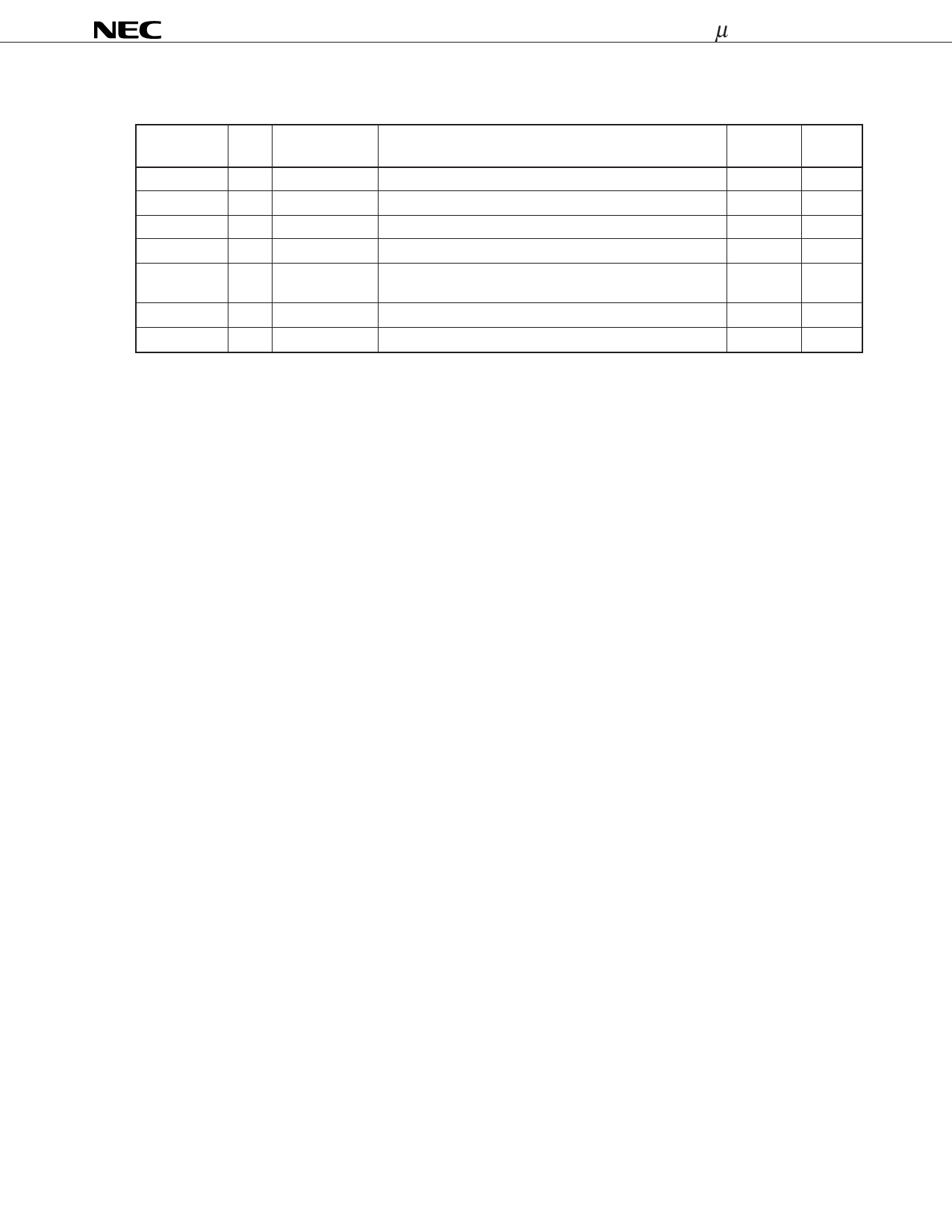
µPD75P3018A
3.2 Non-port Pins (2/2)
Pin Name
I/O Alternate Function
Function
After Reset I/O Circuit
Type
S0-S23
Output
—
Segment signal output
Note 1
G-A
S24-S31
Output BP0-BP7
Segment signal output
Note 1
H-A
COM0-COM3 Output
—
Common signal output
Note 1
G-B
VLC0-VLC2
—
—
Power source for LCD driver
—
—
BIAS
Output
—
Output for external split resistor cut
High
—
impedance
LCDCLNote 2
I/O P30/MD0
Clock output for driving external expansion driver
Input
E-B
SYNCNote 2
I/O P31/MD1
Clock output for synchronization of external expansion driver Input
E-B
Notes 1. The VLCX (X = 0, 1, 2) shown below are selected as the input source for the display outputs.
S0-S31: VLC1, COM0-COM2: VLC2, COM3: VLC0
2. These pins are provided for future system expansion. Currently, only P30 and P31 are used.
Data Sheet U11917EJ2V0DS00
9
Share Link: 