UPD784936A View Datasheet(PDF) - NEC => Renesas Technology
Part Name
Description
Manufacturer
UPD784936A Datasheet PDF : 102 Pages
| |||
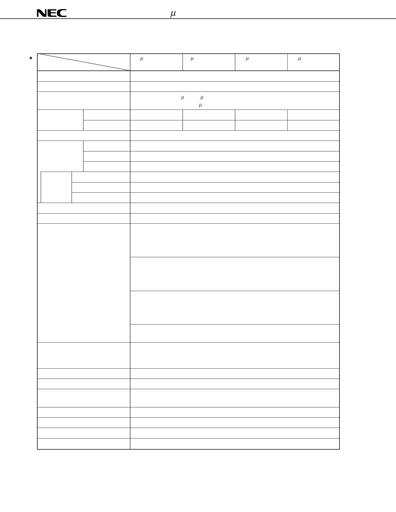
µPD784935A,784936A,784937A,784938A
FUNCTION LIST
(1/2)
Item
Part Number
µPD784935A
µPD784936A
µPD784937A
µPD784938A
Number of basic instructions (mnemonics) 113
General-purpose registers
8 bits × 32 registers × 8 banks, or 16 bits × 8 registers × 8 banks (memory map)
Minimum instruction execution time
320 ns/636 ns/1.27 µs/2.54 µs (@6.29 MHz operation)
160 ns/320 ns/636 ns/1.27 µs (@12.58 MHz operation)
Internal memory ROM
96 KB
128 KB
192 KB
256 KB
RAM
5120 bytes
6656 bytes
8192 bytes
10496 bytes
Memory space
1 MB with program and data spaces combined
I/O port
Total
80 pins
Input
8 pins
I/O
72 pins
Pins with LED direct drive output
ancillary Transistor direct drive
functionNote
N-ch open drain drive
24 pins
8 pins
4 pins
Real-time output port
4 bits × 2, or 8 bits × 1
IEBus controller
Internal (simple version)
Timer/counter
Timer/event counter 0: Timer counter × 1
(16 bits)
Capture register × 1
Compare register × 2
Pulse output possible
• Toggle output
• PWM/PPG output
• One-shot pulse output
Timer/event counter 1:
(16 bits)
Timer counter × 1
Capture register × 1
Capture/compare register × 1
Compare register × 1
Real-time output port
Timer/event counter 2:
(16 bits)
Timer counter × 1
Capture register × 1
Capture/compare register × 1
Compare register × 1
Pulse output possible
• Toggle output
• PWM/PPG output
Timer 3 (16 bits):
Timer counter × 1
Compare register × 1
Watch timer
Generates interrupt request at 0.5-second intervals (internal watch clock oscillator
provided)
Main clock (12.58 MHz) or watch clock (32.7 kHz) selectable as input clock
Clock output
Selectable from fCLK, fCLK/2, fCLK/4, fCLK/8, or fCLK/16 (also usable as 1-bit output port)
PWM output
12-bit resolution × 2 channels
Serial interface
UART/IOE (3-wire serial I/O): 2 channels (with internal baud rate generator)
CSI (3-wire serial I/O):
2 channels
A/D converter
8-bit resolution × 8 channels
Watchdog timer
1 channel
ROM correction function
Internal (4 points of correction addresses can be set.)
External expansion function
Provided (up to 1 MB)
Note Pins with ancillary functions are included in the I/O pins.
4
Data Sheet U13572EJ2V0DS
Share Link: 