USB1T20(2008) View Datasheet(PDF) - Fairchild Semiconductor
Part Name
Description
Manufacturer
USB1T20 Datasheet PDF : 9 Pages
| |||
Pin Configuration
MODE 1
/OE 2
RCV 3
VP 4
VM
5
SUSPND 6
14 VCC
13 VMO/FSEO
12 VPO
11 D+
10 D-
9 SPEED
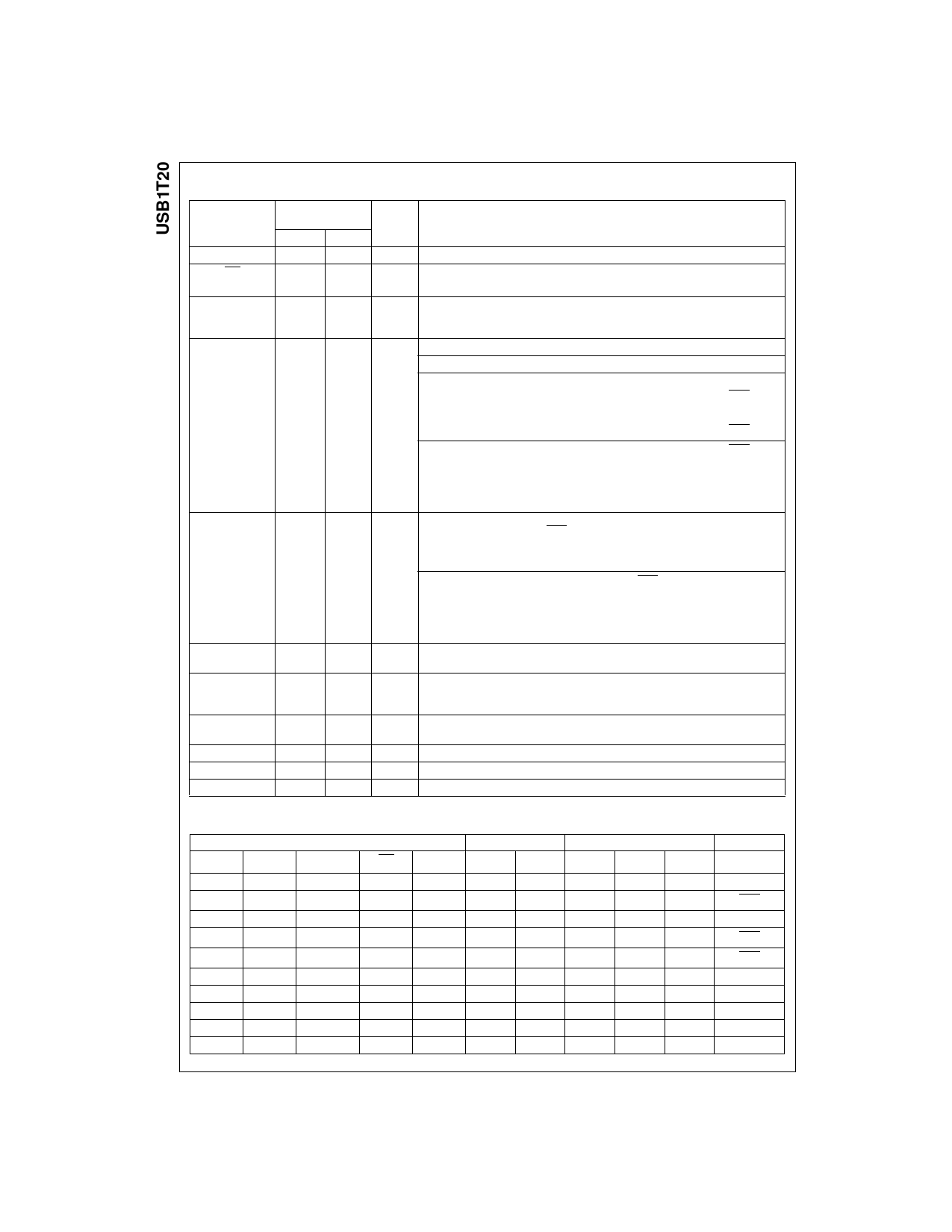
Pin Definitions
Pin #
Name
1
MODE
2
/OE
3
RCV
4, 5
VP,VM
6
7
8
9
10, 11
SUSPND
GND
NC
SPEED
D-, D+
12, 13 VPO,VMO/FSEO
14
VCC
I/O
I
I
O
O
I
I
AI/O
I
GND 7
8 NC
Figure 2. Pin Configuration (Top View)
Description
Mode. When left unconnected, a weak pull-up transistor pulls mode pin to VCC and, in
this GND, the VMO/FSEO pin takes the function of FSEO (force SEO).
Output Enable. Active LOW; enables the transceiver to transmit data on the bus.
When not active, the transceiver is in receive mode.
Receive Data. CMOS-Level output for USB differential input.
Gated version of D- and D+. Outputs are logic “0” and logic “1.” Used to detect single
ended zero (/SEO), error conditions, and interconnected speed. (Input to SIE).
VP
VM
RESULT
0
0
/SEO
0
1
Low Speed
1
0
Full Speed
0
1
Error
Suspend. Enables a low-power state while the USB bus is inactive. While the
suspend pin is active, it drives the RCV pin to a logic “0” state. Both D+ and D- are 3-
state.
Ground reference.
No connect.
Edge Rate Control. Logic “1” operates at edge rates for full speed. Logic “0” operates
edge rates for low speed.
Data+, Data-. Differential data bus conforming to the Universal Serial Bus standard.
Inputs to differential driver. (Outputs from SIE.)
Mode
VPO
VMO/FSEO
RESULT
0
0
Logic “0”
0
1
/SEO
0
1
0
Logic “1”
1
1
/SEO
0
0
/SEO
0
1
Logic “0”
1
1
0
Logic “1”
1
1
Illegal Code
3.0 to 3.6 power supply.
© 2004 Fairchild Semiconductor Corporation
USB1T20 • Rev. 1.0.2
2
www.fairchildsemi.com
Share Link: 