VN610SP-E View Datasheet(PDF) - STMicroelectronics
Part Name
Description
Manufacturer
VN610SP-E Datasheet PDF : 18 Pages
| |||
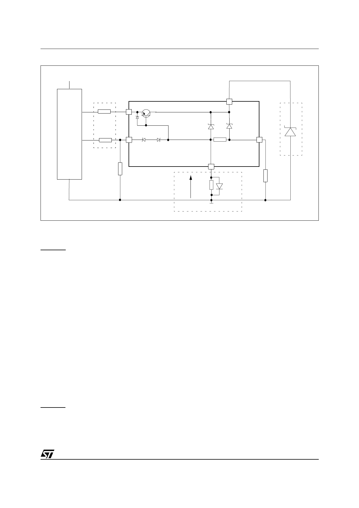
Figure 8. Application Schematic
+5V
Rprot
INPUT
VCC
µC
Rprot
CURRENT SENSE
RSENSE
GND
OUTPUT
RGND
VGND
DGND
VN610SP-E
Dld
GND PROTECTION NETWORK AGAINST
REVERSE BATTERY
Solution 1: Resistor in the ground line (RGND only). This
can be used with any type of load.
The following is an indication on how to dimension the
RGND resistor.
1) RGND ≤ 600mV / (IS(on)max).
2) RGND ≥ (−VCC) / (-IGND)
where -IGND is the DC reverse ground pin current and can
be found in the absolute maximum rating section of the
device’s datasheet.
Power Dissipation in RGND (when VCC<0: during reverse
battery situations) is:
PD= (-VCC)2/RGND
This resistor can be shared amongst several different
HSD. Please note that the value of this resistor should be
calculated with formula (1) where IS(on)max becomes the
sum of the maximum on-state currents of the different
devices.
Please note that if the microprocessor ground is not
common with the device ground then the RGND will
produce a shift (IS(on)max * RGND) in the input thresholds
and the status output values. This shift will vary
depending on how many devices are ON in the case of
several high side drivers sharing the same RGND.
If the calculated power dissipation leads to a large
resistor or several devices have to share the same
resistor then the ST suggests to utilize Solution 2 (see
below).
Solution 2: A diode (DGND) in the ground line.
A resistor (RGND=1kΩ) should be inserted in parallel to
DGND if the device will be driving an inductive load.
This small signal diode can be safely shared amongst
several different HSD. Also in this case, the presence of
the ground network will produce a shift (j600mV) in the
input threshold and the status output values if the
microprocessor ground is not common with the device
ground. This shift will not vary if more than one HSD
shares the same diode/resistor network.
Series resistor in INPUT line is also required to prevent
that, during battery voltage transient, the current exceeds
the Absolute Maximum Rating.
Safest configuration for unused INPUT pin is to leave it
unconnected, while unused SENSE pin has to be
connected to Ground pin.
LOAD DUMP PROTECTION
Dld is necessary (Voltage Transient Suppressor) if the
load dump peak voltage exceeds VCC max DC rating.
The same applies if the device will be subject to
transients on the VCC line that are greater than the ones
shown in the ISO T/R 7637/1 table.
µC I/Os PROTECTION:
If a ground protection network is used and negative
transients are present on the VCC line, the control pins will
be pulled negative. ST suggests to insert a resistor (Rprot)
in line to prevent the µC I/Os pins to latch-up.
The value of these resistors is a compromise between the
leakage current of µC and the current required by the
HSD I/Os (Input levels compatibility) with the latch-up
limit of µC I/Os.
-VCCpeak/Ilatchup ≤ Rprot ≤ (VOHµC-VIH-VGND) / IIHmax
Calculation example:
For VCCpeak= - 100V and Ilatchup ≥ 20mA; VOHµC ≥ 4.5V
5kΩ ≤ Rprot ≤ 65kΩ.
Recommended Rprot value is 10kΩ.
9/18
Share Link: 