VN920PEP-E(2013) View Datasheet(PDF) - STMicroelectronics
Part Name
Description
Manufacturer
VN920PEP-E Datasheet PDF : 26 Pages
| |||
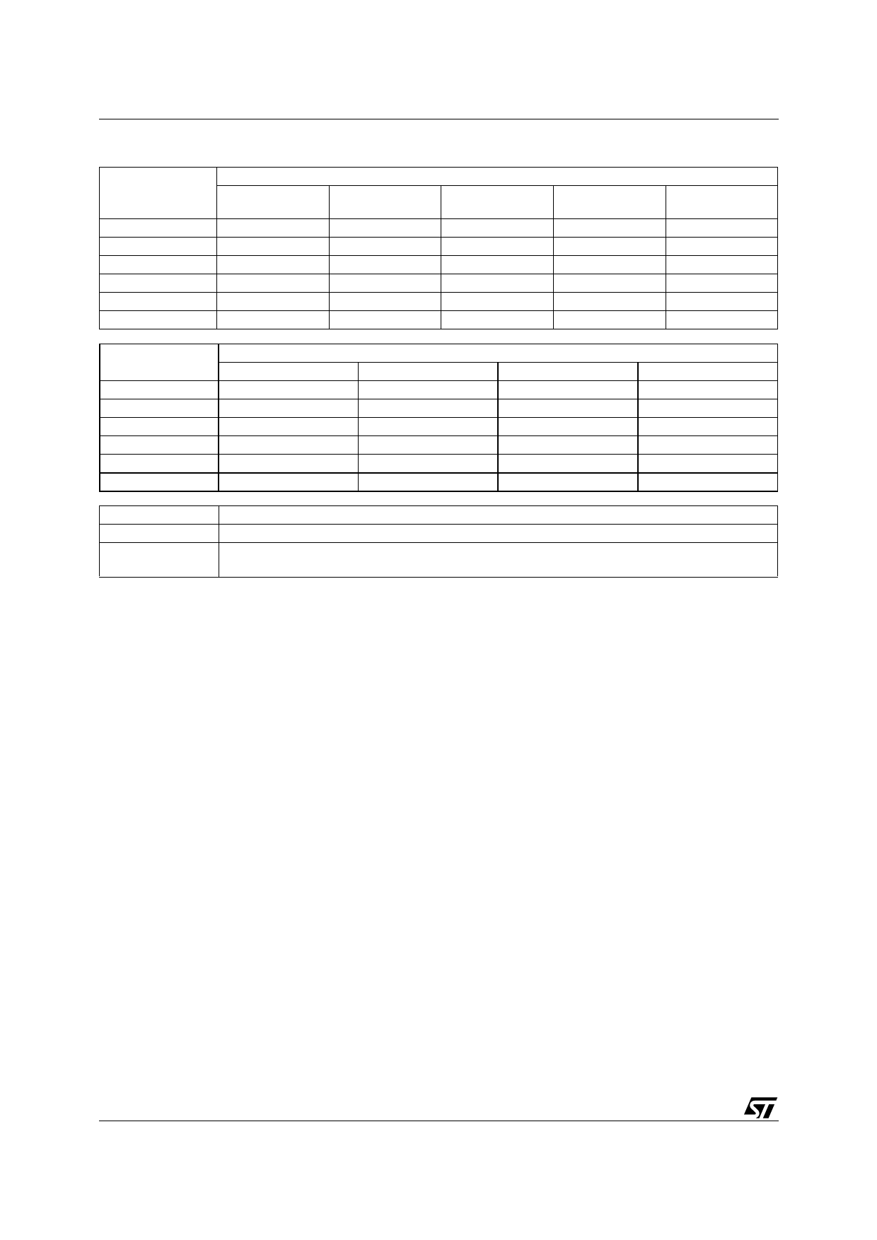
Electrical specifications
VN920PEP-E
Table 5.
Symbol
Power (continued)
Parameter
Test conditions
Off-state; VCC = 13V;
VIN = VOUT = 0V
Min. Typ. Max. Unit
10 25 µA
IS Supply current
Off-state; VCC = 13V;
VIN = VOUT = 0V; Tj = 25°C
10 20 µA
On-state; VCC = 13V; VIN = 5V;
IOUT = 0A; RSENSE = 3.9 k
5 mA
IL(off1) Off-state output current VIN = VOUT = VSENSE= 0V
t(s) IL(off3)
Off-state output current
VIN = VOUT = VSENSE = 0V;
VCC = 13V; Tj = 125°C
duc IL(off4)
Off-state output current
VIN = VOUT = VSENSE = 0V;
VCC = 13V; Tj = 25°C
ro 1. Vclamp and VOV are correlated. Typical difference is 5V.
te P Table 6. Switching (VCC=13V)
le Symbol
Parameter
Test conditions
so td(on)
Turn-on delay time RL = 1.3(see Figure 5)
Ob td(off)
Turn-off delay time RL = 1.3(see Figure 5)
- dVOUT/dt(on) Turn-on voltage slope RL = 1.3(see Figure 5)
t(s) dVOUT/dt(off) Turn-off voltage slope RL = 1.3(see Figure 5)
uc Table 7. Logic inputs
rod Symbol
Parameter
P VIL
teIIL
ole VIH
bs IIH
O VI(hyst)
Input low level voltage
Low level input current
Input high-level voltage
High-level input current
Input hysteresis voltage
Test conditions
VIN = 1.25V
VIN = 3.25V
0
50 µA
5 µA
3 µA
Min. Typ. Max. Unit
50
50
See Figure 16
See Figure 17
µs
µs
V/µs
V/µs
Min. Typ. Max. Unit
1.25 V
1
µA
3.25
V
10 µA
0.5
V
VICL Input clamp voltage
IIN = 1mA
IIN = - 1mA
6
6.8
8
V
- 0.7
V
8/26
Doc ID 10874 Rev 7
Share Link: 