W523S25 View Datasheet(PDF) - Winbond
Part Name
Description
Manufacturer
W523S25 Datasheet PDF : 14 Pages
| |||
W523SXX (PRELIMINARY)
power-on, an “ END” instruction should be entered in the group 32.
The interruption priority is shown as below while other trigger pins as well as JUMP (JP) command are
executing simultaneously during POI executing period:
POI > TG1F > TG1R > TG2F > TG2R > TG5F > TG5R > TG6F > TG6R > "JP" instruction.
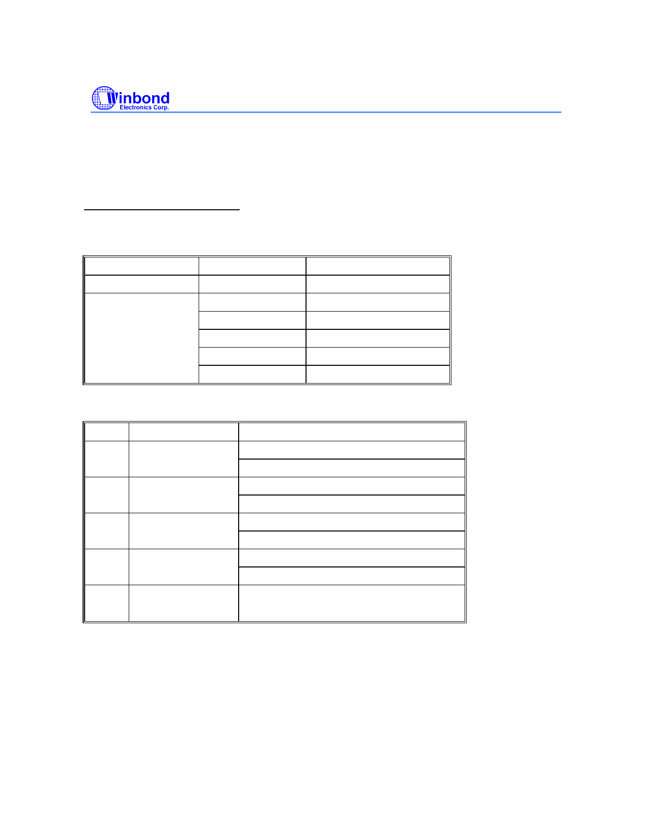
Register Definition and Control
The register file in the W523Sxx family is composed of 10 registers, including 4 general-purpose
registers and 6 special purpose registers. They are defined to facilitate the operations for various
purposes. The default setting values of the registers are given in the following table.
REGISTER
NAME
DEFAULT SETTING
General Register
R0-R3
00100000B
Special Register
EN0
XX11XX11B
EN1
XX11XX11B
MODE0, MODE1
11111111B
STOP
XXX11111B
PAGE
00000000B
1. MODE0 Register
BIT
DESCRIPTION
7 LED mode
6 LED2/STPC
pin selection
4 Debounce time
2 STPA/BUSY
pin selection
5,3,1,0 X
DEFINITION
1: Flash
0: DC
1: LED2 output
0: STPC output
1: Long
0: Short
1: STPA output
0: BUSY output
Don’ t care
The MODE0.7 bit defines the output type of LED1 and LED2 pins as Flash output (3 Hz) or DC output.
The MODE0.6 bit defines the configuration of LED2/STPC pin’ s status as LED2 output or STPC
output. The MODE0.4 bit defines the trigger pin’ s debounce time as long debounce (50 mS) or short
debounce (400 uS). The MODE0.2 bit defines the behavior of the STPA/BUSY pin as STPA output in
normal mode or BUSY signal output in CPU mode. The bits 5, 3, 1 and 0 are don’ t care bits.
-4-
Share Link: 