W523S99 View Datasheet(PDF) - Winbond
Part Name
Description
Manufacturer
W523S99 Datasheet PDF : 14 Pages
| |||
W523SXX (PRELIMINARY)
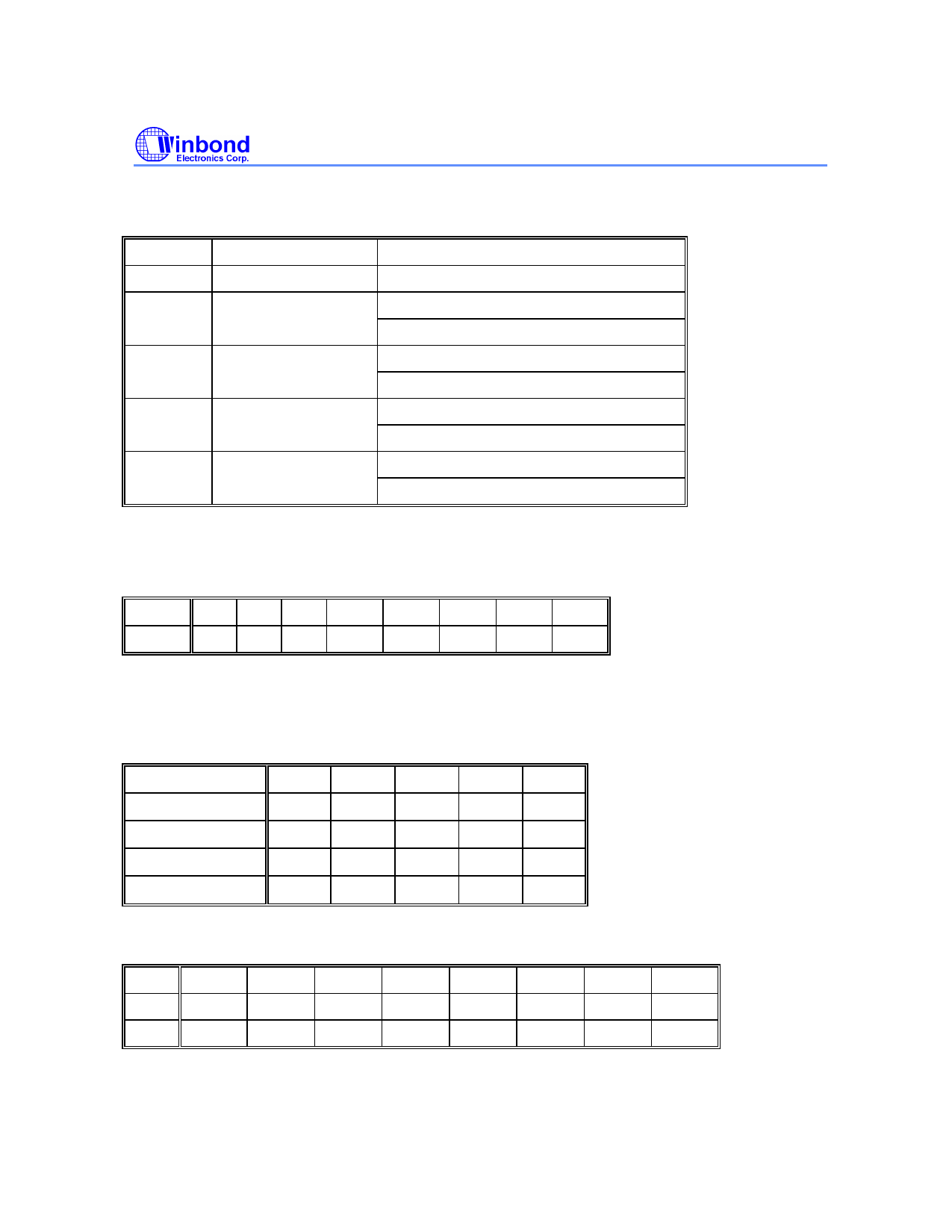
2. MODE1 Register
BIT
7, 6, 1, 0
5
DESCRIPTION
X
LED Flash type
4
LED1 section
control
3
LED2 control
2
LED1 volume
control
DEFINITION
Don’ t care
1: Alternate
0: Synchronous
1: YES
0: NO
1: SECTION control
0: STPC control
1: OFF
0: ON
MODE1.5 is for LED flash type control. MODE1.4 is for LED1 section control ON/OFF. MODE1.3 is for
LED2 Section/STPC control. MODE1.2 is for LED1 volume control.
3. PAGE Register
BIT
765
4
3
2
1
0
PAGE -
-
-
PG4 PG3 PG2 PG1 PG0
The bits 0 ~ 4 in PAGE register are used for page selection. Once the page mode being defined
(referring to the below section of “Option Control Function”), the working page is selected by the bits 0
~ 4 in the PAGE register. Hence, the user can execute "LD PAGE, value" instruction to change the
working page of the voice entry group. Not all of the bits 0 ~ 4 of PAGE register are used in different
page mode. They are listed as below table:
PAGE MODE PG4 PG3 PG2 PG1 PG0
1-page
8-page
16-page
32-page
×
×
×
×
×
×
×
√
√
√
×
√
√
√
√
√
√
√
√
√
Where "×" means don′t care and "√" means must be set properly.
4. EN Register
BIT
7
6
5
4
3
2
EN0
X
X
TG2R TG1R
X
X
EN1
X
X
TG6R TG5R
X
X
1
TG2F
TG6F
0
TG1F
TG5F
EN0 or EN1 is an 8-bit register that stores the rising/falling edge enable or disable status information
for all trigger pins, which determines whether each trigger pin is retriggerable, non-retriggerable,
Publication Release Date: Oct 2000
-5-
Revision A5
Share Link: 