WCMC1616V9X View Datasheet(PDF) - Weida Semiconductor, Inc.
Part Name
Description
Manufacturer
WCMC1616V9X Datasheet PDF : 13 Pages
| |||
ADVANCE INFORMATION
WCMC1616V9X
Features
• 1T Cell, PSRAM Architecture
• High speed: 70 ns
• Wide Voltage range:
— VCC range: 2.7V to 3.3V
• Low active power
— Typical active current: 2 mA @ f = 1 MHz
— Typical active current: 13 mA @ f = fMAX
• Low standby power
• Automatic power-down when deselected
Functional Description[1]
The WCMC1616V9X is a high-performance CMOS pseudo
static RAMs (PSRAM) organized as 1M words by 16 bits that
supports an asynchronous memory interface. This device
features advanced circuit design to provide ultra-low active
current. This is ideal for providing More Battery LifeTM
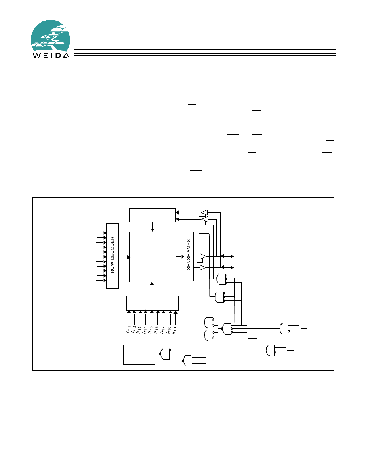
Logic Block Diagram
1Mb x 16 Pseudo Static RAM
(MoBL®) in portable applications such as cellular telephones.
The device can be put into standby mode reducing power
consumption by more than 99% when deselected using CE
LOW, CE 2 HIGH or both BHE and BLE are HIGH. The
input/output pins (I/O0 through I/O15) are placed in a
high-impedance state when: deselected (CE HIGH, CE 2 LOW
OE is deasserted HIGH), or during a write operation (Chip
Enabled and Write Enable WE LOW). The device also has an
automatic power-down feature that significantly reduces
power consumption by 99% when addresses are not toggling
even when the chip is selected (Chip Enable CE LOW, CE 2
HIGH and both BHE and BLE are LOW). Reading from the
device is accomplished by asserting the Chip Enables (CE
LOW and CE 2 HIGH) and Output Enable (OE) LOW while
forcing the Write Enable (WE) HIGH. If Byte Low Enable (BLE)
is LOW, then data from the memory location specified by the
address pins will appear on I/O0 to I/O7. If Byte High Enable
(BHE ) is LOW, then data from memory will appear on I/O8 to
I/O15. See the Truth Table for a complete description of read
and write modes.
DATA IN DRIVERS
A10
A9
A8
A7
A6
1M x 16
A5
A4
RAM Array
A3
1T
A2
A1
A0
I/O0–I/O7
I/O8–I/O15
COLUMN DECODER
Power -Down
Circuit
BHE
BLE
BHE
WE
OE
BLE
CE2
CE
CE2
CE
Note:
1. For best-practice recommendations, please refer to the Cypress application note “System Design Guidelines” on http://www.cypress .com.
WeidaSemiconductor, Inc.
Document #: 38-14027 Rev. **
Revised August 22, 2001
Share Link: 