DSP16410C View Datasheet(PDF) - Agere -> LSI Corporation
Part Name
Description
Manufacturer
DSP16410C Datasheet PDF : 373 Pages
| |||

This document, the DSP16410B Digital Signal Processor Data Sheet (DS01-070WINF) replaces the
DSP16410 Digital Signal Processor Data Sheet (DS98-318WTEC) dated July 2000 and the DSP16410B
Digital Signal Processor Data Addendum (DA00-014WTEC) dated July 2000. This new document is the
complete specification for the DSP16410B device and no longer specifies the discontinued DSP16410A
device. The following table summarizes the changes to the information in this data sheet since July 2000.
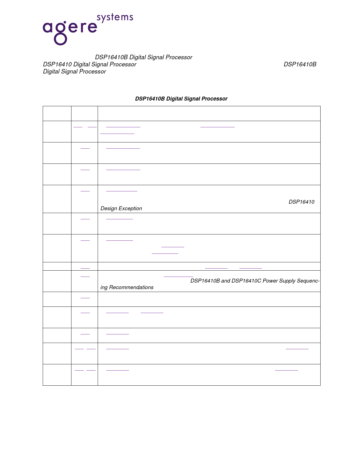
Significant Changes to the DSP16410B Digital Signal Processor Data Sheet Since July 2000
Old
New
Page(s) Page(s)
Change
155—157 156—158 In Section 4.16.3, Basic Input Processing, Section 4.16.4, Basic Output Processing, and
Section 4.16.5, Clock and Frame Sync Generation, notes were added to specify that the com-
bination of passive bit clock and active frame sync is not supported.
156
157 In Section 4.16.4, Basic Output Processing, it now states “If an output bit clock is active (inter-
nally generated), the user program must wait at least four bit clock cycles between changing
AGRESET (SCON12[15]) and clearing ORESET.” (changed from two bit clock cycles).
164
165 In Section 4.16.8, Basic Frame Structure, a note was added that specifies that if the output
section is configured for a one-channel frame and a passive frame sync, the SOFS frame
sync interval must be constant and a multiple of the OCK output bit clock.
225
224 In Section 6.2.1, Directly Program-Accessible (Register-Mapped) Registers, text was added
that explains that off-core register-mapped registers cannot be stored to memory in a single
instruction. This is due to a design exception that was described in the advisory DSP16410
Design Exception (AY01-004WTEC).
265
263 In Section 8.6, PIU Interface, the description of the PCSN pin had incorrectly stated that if
PCSN = 1, the PIU 3-states POBE, PIBF, PRDY, and PINT. This has been corrected to state
that the PIU 3-states only PD[15:0].
267
265 In Section 9.1, Absolute Maximum Ratings, the maximum solder temperature was changed
from 300 °C to 220 °C. In Table 175, the minimum storage temperature was changed from
–65 °C to –40 °C. In Section 9.2, Handling Precautions, the breakdown voltage was
changed from 2000 V to 1000 V.
270
268 The ranges for IOH and IOL were changed in Figure 63 and Figure 64, respectively.
—
273 A new section was added: Section 10.4, Power Supply Sequencing Issues. This information
had been documented in the advisory DSP16410B and DSP16410C Power Supply Sequenc-
ing Recommendations (AY01-002WTEC).
274
276 The temperature range conditions listed for the timing characteristics had been for ambient
temperature (TA) and are now for junction temperature (TJ = –40 °C to +120 °C).
285
287 In Figure 77 and Table 198 that describe the SEMI asynchronous read timing, the t94 specifi-
cation (External Memory Access Time) has been deleted. Instead, a note was added that the
external memory access time can be calculated as t90 – (t91 + t92).
286
288 In Table 200, Timing Characteristics for Asynchronous Memory Write Operations, the specifi-
cation for t100 has been moved from the “Max” column to the “Min” column.
288, 289 289, 290 In Table 202, Timing Characteristics for Synchronous Read Operations, and in Table 203,
Timing Characteristics for Synchronous Write Operations, the value for the t106 specification
was changed from 0.5 ns to 2.5 ns.
298, 299 300, 301 In Table 220, Timing Requirements for SIU Active Frame Mode Input, and Table 222, Timing
Requirements for SIU Active Channel Mode Input, the value for the t49 specification was
changed from 5 ns to 9 ns.