LC83026E View Datasheet(PDF) - SANYO -> Panasonic
Part Name
Description
Manufacturer
LC83026E Datasheet PDF : 16 Pages
| |||
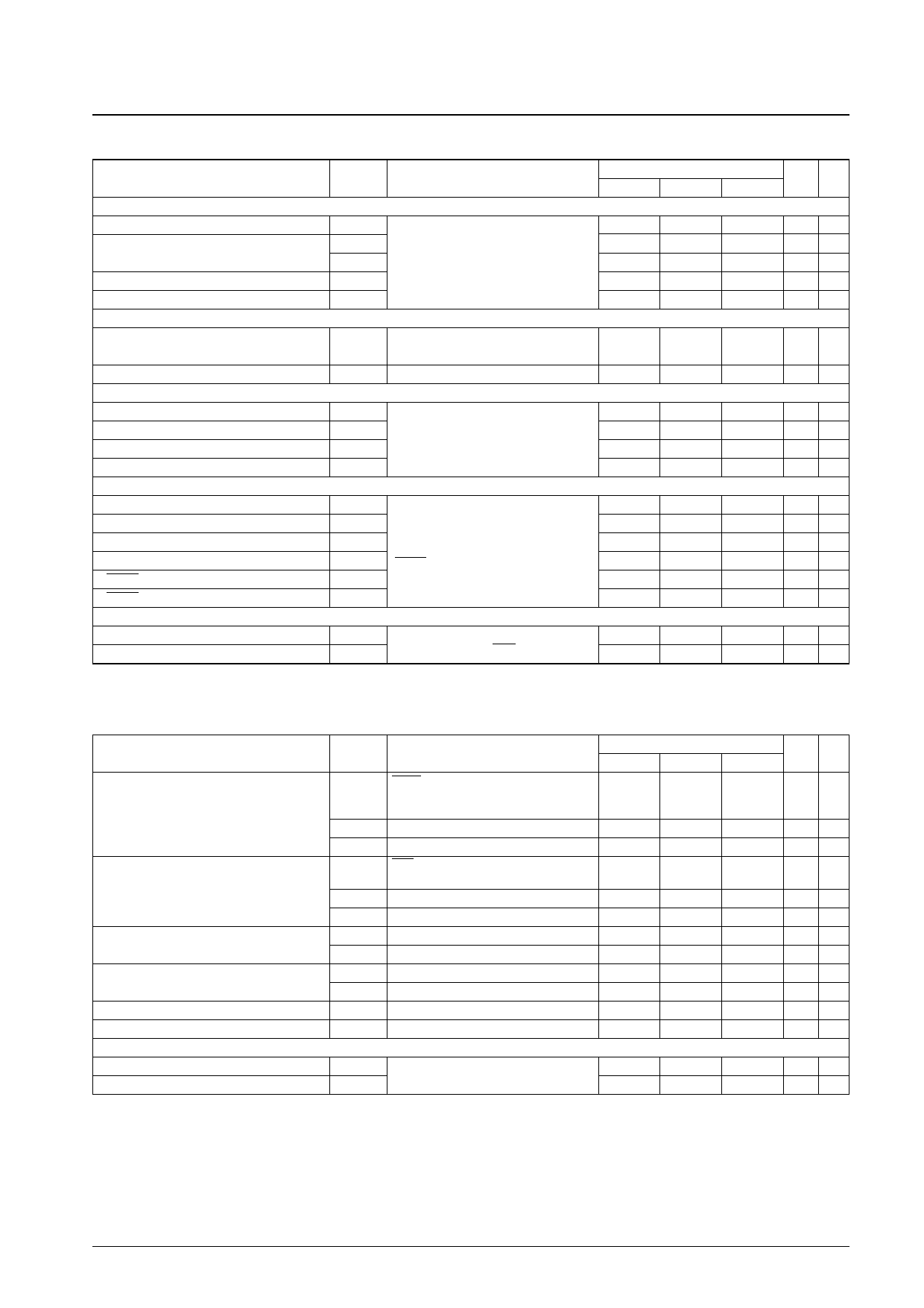
LC83026E
Continued from preceding page.
Parameter
Symbol
Conditions
[External Clock Input Conditions]
Frequency
fEXT
Pulse width
fEXTH
fEXTL
Rise time
tEXTR
Fall time
tEXF
[Self-Excited Oscillation Conditions(crystal oscillator)]
Oscillator frequency
fOSC
Oscillator stabilization period
[Audio Data Input Conditions]
Transfer bit clock period
Transfer bit clock pulse width
Data setup time
Data hold time
[Serial I/O Clock Conditions]
Serial clock period
Serial clock pulse width
Data setup time
Data hold time
SRDY hold time
SRDY pulse width
[DRAM Input Conditions]
Input data setup time
Input data hold time
tOSCS
tBCYC
tBCW
tS
tH
tSCYC
tSCW
tSS
tSH
tSYH
tSYW
tDSI
tDHI
Related to the FS384I pin. See Figure 1.
maximum: 44.1 kHz × 384 × 1.005
minimum: 44.1 kHz × 384 × 0.995
OSC1 and OSC2. See Figure 2.
44.1 kHz/48 kHz × 768 ±0.1%
See Figure 3.
Related to BCKI. See Figure 4.
Related to the microcontroller interface.
See Figure 5. (Related to SICK, SI, and
SRDY.)
Related to external DRAM data input. See
Figure 6. (Related to CAS and D0 to D7.)
Ratings
min
typ
16.85
23
23
33.84
354
100
70
70
480
200
70
70
200
200
20
0
Unit Notes
max
17.01
9
9
MHz
ns
ns
ns
ns
40.55 MHz
100 ms
ns
ns
ns
ns
ns
ns
ns
ns
ns
ns
ns
ns
Electrical Characteristics 1 at Ta = –30 to +70°C, all VDD = 4.75 to 5.25 V, all VSS = 0 V unless otherwise specified
Parameter
Input high-level current
Input low-level current
Output high-level voltage
Output low-level voltage
Output off leakage current
Input and output capacitance
[Audio Data Output Timing]
Output data hold time
Output data delay time
Symbol
IIH1
IIH2
IIH3
IIL1
IIL2
IIL3
VOH1
VOH2
VOL1
VOL2
IOFF
CIO
Conditions
SELC, SAIF, SAOF,
VIN = VDD (Input pins with pull-down
resistors)
P0 to P2, VIN = VDD (Nch transistor OFF)
Other input-only pins
RES, VIN = VSS (Input pins with pull-up
resistors)
P0 to P2, VIN = VSS
Other input-only pins
IOH = –0.4 mA
IOH = –50 µA
IOL = 2 mA
IOL = 10 mA
VO = VSS, VDD
min
–250
–10
–10
4.0
VDD –1.2
–40
Ratings
typ
100
–100
4.98
4.997
0.065
0.32
Unit Notes
max
250 µA 8
10 µA
10 µA
µA 8
µA
µA
V 1, 8
V 2,3,8
0.4 V 1, 8
1.5 V 2,3,8
+40 µA
10 pF
tOH
BCK0 and ASO. See Figure 7.
tOD
–30
ns 7
50 ns 7
Continued on next page.
No. 5663-6/16
Share Link: 