ADV7175 View Datasheet(PDF) - Analog Devices
Part Name
Description
Manufacturer
ADV7175 Datasheet PDF : 36 Pages
| |||
ADV7175/ADV7176
(Continued from page 1)
The ADV7175/ADV7176 also supports both a PAL and NTSC
square pixel mode in slave mode.
The video encoder accepts an 8-bit parallel pixel data stream in
CCIR-656 format or a 16-bit parallel data stream. This 4:2:2
data stream is interpolated into 4:4:4 component video (YUV).
The YUV video is interpolated to two times the pixel rate. The
color-difference components (UV) are quadrature modulated
using a subcarrier frequency generated by an on-chip synthesizer
(also running at two times the pixel rate). The two times pixel
rate sampling allows more accurate generation of the subcarrier
because frequency and phase errors are reduced by the higher
sampling rate. The ADV7175/ADV7176 also offers the option to
output the YUV information directly.
The luminance and chrominance components are digitally com-
bined and the resulting composite signal is output via a 10-bit
DAC. Three additional 10-/8-bit DACs are provided to output
S-VHS Y/C Video (10 bits), YUV or RGB Video (8 bits).
The output video frames are synchronized with the incoming
data timing reference codes. Optionally the encoder accepts (and
can generate) HSYNC, VSYNC & FIELD timing signals. These
timing signals can be adjusted to change pulse width and posi-
tion while the part is in the master mode. The encoder requires a
single two times pixel rate (27 MHz) clock for standard operation.
Alternatively the encoder requires 24.54 MHz clock for NTSC
or 29.5 MHz clock for PAL square pixel mode operation. All in-
ternal clocks are generated on-chip. The ADV7175/ADV7176
modes are set up over a two wire serial bidirectional port (I2C
Compatible) with two slave addresses.
Additionally, the ADV7175/ADV7176 allows a subcarrier phase
lock with an external video source and has a color bar generator
on-board.
Functionally the ADV7175 and ADV7176 are the same with
the exception that the ADV7175 can output the Macrovision
(Revision 6.1/7.x) anticopy algorithm.
The ADV7175/ADV7176 is fabricated in a +5 V CMOS pro-
cess. Its monolithic CMOS construction ensures greater func-
tionality with low power dissipation.
The ADV7175/ADV7176 is packaged in a 44-pin thermally en-
hanced PQFP package (patent pending).
The ADV7175/ADV7176 is protected by U.S. Patent Numbers
5,343,196 and 5,442,355 and other intellectual property rights.
DATA PATH DESCRIPTION
For PAL B, D, G, H, I, M, N and NTSC M, N modes, YCrCb
4:2:2 data is input via the CCIR-656 compatible pixel port at a
13.5 MHz data rate. The pixel data is de-multiplexed to form
three data paths. Y has a range of 16 to 235, Cr and Cb have a
range of 128 ± 112. The ADV7175/ADV7176 supports PAL
(B, D, G, H, I, N, M) and NTSC (with and without Pedestal)
standards. The appropriate SYNC, BLANK and burst levels are
added to the YCrCb data. Macrovision antitaping (ADV7175
only) and close-captioning levels are also added to Y and the
resultant data is interpolated to a rate of 27 MHz. The interpo-
lated data is filtered and scaled by three digital FIR filters.
The U and V signals are modulated by the appropriate subcarrier
sine/cosine phases and added together to make up the chromi-
nance signal. The luma (Y) signal can be delayed 1-3 luma
cycles (each cycle is 74 ns) with respect to the chroma signal.
The luma and chroma signals are then added together to make
up the composite video signal. All edges are slew rate limited.
The YCrCb data is also used to generate RGB data with appro-
priate SYNC and BLANK levels. The RGB data is in sychro-
nization with the composite video output. Alternatively analog
YUV data can be generated instead of RGB.
The four 10-bit DACs can be used to output:
1. 10-bit composite video + 8-bit RGB video.
2. 10-bit composite video + 8-bit YUV video.
3. Two 10-bit composite video signals
+ 10-bit LUMA & CHROMA (Y/C) signals.
Alternatively, each DAC can be individually powered off if not
required.
All possible video outputs are illustrated in Appendix 3, 4 and 5.
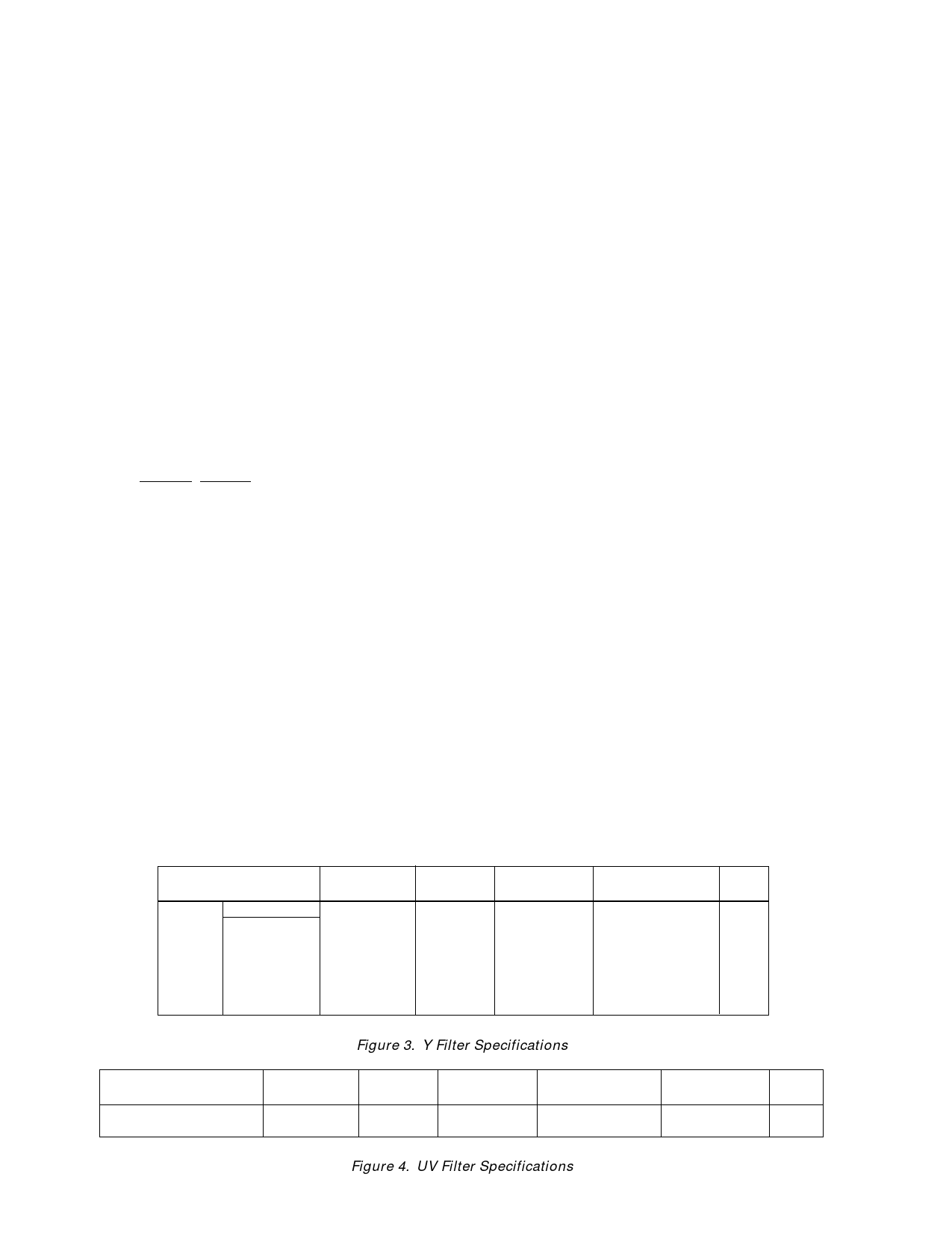
INTERNAL FILTER RESPONSE
The Y filter supports several different frequency responses in-
cluding two 4.5/5.0 MHz low-pass and PAL/NTSC subcarrier
notch responses. The U and V filters have a 0.6/1 0.3 MHz
low-pass response.
These filter characteristics are illustrated in Figures 3 to 11.
FILTER SELECTION
NTSC
PAL
NTSC
PAL
NTSC/PAL
NTSC
PAL
MR04
0
0
0
0
1
1
1
MR03
0
0
1
1
0
1
1
PASSBAND
PASSBAND
STOPBAND
CUT OFF (MHz) RIPPLE (dB) CUT OFF (MHz)
2.3
0.026
7.5
3.4
0.098
8.0
1.0
0.085
3.57
1.4
0.107
4.43
4.0
0.150
8.0
2.3
0.054
7.5
3.4
0.106
8.0
STOPBAND
ATTENUATION (dB)
>50
>51.3
>27.6
>29.3
>40
>54
>50.3
F3dB
4.2
5.0
2.1
2.7
5.65
4.2
5.0
FILTER SELECTION
NTSC
PAL
Figure 3. Y Filter Specifications
PASSBAND
CUT OFF (MHz)
1.0
1.3
PASSBAND
RIPPLE (dB)
0.085
0.04
STOPBAND
CUT OFF (MHz)
3.6
4.0
STOPBAND
ATTENUATION (dB)
>40
>40
ATTENUATION @
1.3MHz (dB)
0.3
0.02
F3dB
2.05
2.45
Figure 4. UV Filter Specifications
–6–
REV. A
Share Link: 