YSS950 View Datasheet(PDF) - Yamaha Corporation
Part Name
Description
Manufacturer
YSS950 Datasheet PDF : 30 Pages
| |||
YSS950
Type
Power supply
Pin Pin Name I/O
Function
No.
Note 1)
26 VDD33 −
Digital power supply for pin block (Typ. 3.3 V)
39
55
9 VDD12 −
24
Digital power supply for Core block (Typ. 1.2 V)
25
40
41
56
57
62 PAVDD −
64
Power supply for PLL analog block (Typ. 1.2 V)
Insert a 0.1 µF capacitor between the PAVDD and PAVSS pins.
3 PDVDD −
Power supply for PLL digital block (Typ. 1.2 V)
Insert a 0.1 µF capacitor between the PDVDD and PDVSS pins.
4 VSS
16
−
Digital ground
17
32
33
48
49
61
1 PAVSS −
63
PLL analog ground
Insert a 0.1 µF capacitor between the PAVDD and PAVSS pins.
2 PDVSS −
PLL digital ground
Insert a 0.1 µF capacitor between the PDVDD and PDVSS pins.
Note 1)
• I:
• Is:
• I+:
• O:
• Ot:
I/O symbols
Input
Schmitt trigger input
Built in pull-up circuit (*)
Output
3-state output
* Built in pull-up circuit cannot be used for Hi-level output of the LSI, because of this ability is only keep Hi-level for input pin
when it is open.
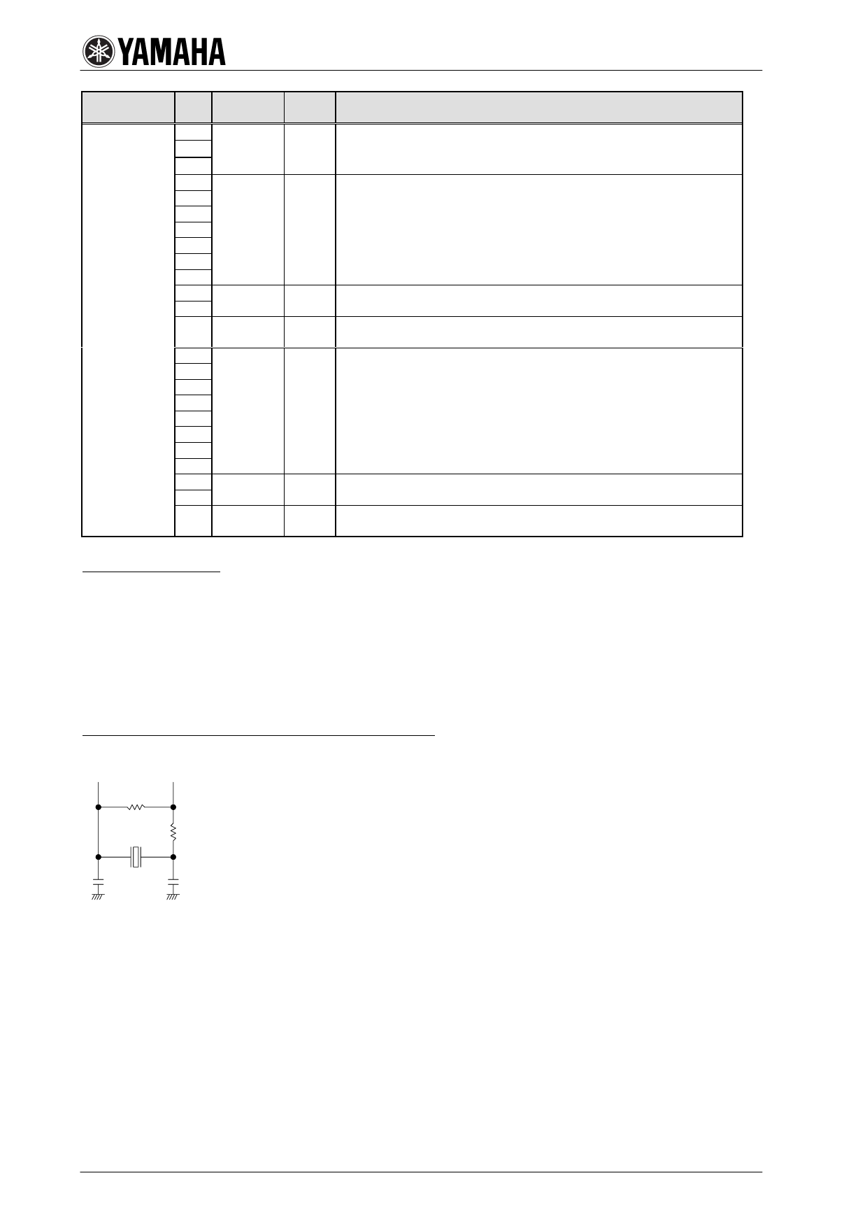
Note 2) Example of circuit connected to crystal oscillator
XI
XO
12.288 MHz
* The above resistor and capacitor values vary depending on a crystal oscillator. Be sure to meet the
specifications for the crystal oscillator to be used.
8
Share Link: 