Z89C00 View Datasheet(PDF) - Zilog
Part Name
Description
Manufacturer
Z89C00 Datasheet PDF : 28 Pages
| |||
ZILOG
RAM ADDRESSING (Continued)
PRELIMINARY
Z89C00
16-BIT DIGITAL SIGNAL PROCESSOR
The register pointer is specified by the first and second bits
in the source/destination field and the modification is
specified by the third and fourth bits according to the
following table:
D3-D0
Meaning
00xx
01xx
10xx
11xx
NOP
+1
–1/LOOP
+1/LOOP
No Operation
Simple Increment
Decrement Modulo the Loop Count
Increment Modulo the Loop Count
xx00
xx01
xx10
xx11
P0:0 or P0:1
P1:0 or P1:1
P2:0 or P2:1
See Note a.
See Note a.
See Note a.
See Short Form Direct
Note:
a. If bit 8 is zero, P0:0 to P2:0 are selected; if bit 8 is one, P0:1 to P2:1
are selected.
When Loop mode is selected, the pointer to which the loop
is referring will cycle up or down, depending on whether a
–LOOP or +LOOP is specified. The size of the loop is
obtained from the least significant three bits of the Status
Register. The increment or decrement of the register is
accomplished modulo the loop size. As an example, if the
loop size is specified as 32 by entering the value 101 into
bits 2-0 of the Status Register (S2-S0) and an increment
+LOOP is specified in the address field of the instruction,
i.e., the RPi field is 11xx, then the register specified by RPi
will increment, but only the least significant five bits will be
affected. This means the actual value of the pointer will
cycle round in a length 32 loop, and the lowest or highest
value of the loop, depending on whether the loop is up or
down, is set by the three most significant bits. This allows
repeated access to a set of data in RAM without software
intervention. To clarify, if the pointer value is 10101001 and
if the LOOP = 32, the pointer increments up to 10111111,
then drops down to 10100000 and starts again. The upper
three bits remaining unchanged. Note that the original
value of the pointer is not retained.
2. Direct Register
The second method is a direct addressing method.
The address of the RAM is directly specified by
the address field of the instruction. Because this
addressing method consumes nine bits (0-511) of the
instruction field, some instructions cannot use this
mode (Figure 6).
Figures 8 to 13 show the different register instruction
formats along with the two tables below Figure 8.
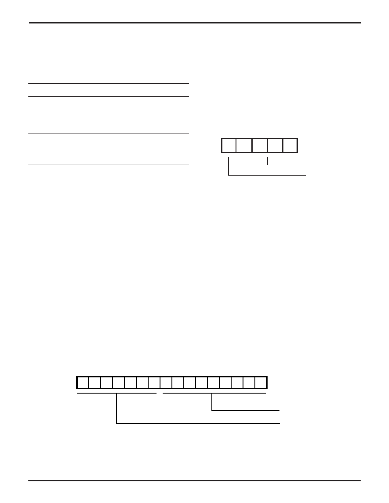
b n3 n2 n1 n0
D8 S3 S2 D3 D2
RAM Address
RAM Bank
Figure 7. Short Form Direct Address
3. Short Form Direct
Dn:b n = 0-3, b = 0-1
The last method is called Short Form Direct Addressing,
where one out of 32 addresses in internal RAM can be
specified. The 32 addresses are the 16 lower addresses
in RAM Bank 0 and the 16 lower addresses in RAM
Bank 1. Bit 8 of the instruction field determines RAM
Bank 0 or 1. The 16 addresses are determined by a
4-bit code comprised of bits S3 and S4 of the status
register and the third and fourth bits of the Source/
Destination field. Because this mode can specify a
direct address in a short form, all of the instructions
using the register indirect mode can use this mode
(Figure 7). This method can access only the lower 16
addresses in the both RAM banks and as such has
limited use. The main purpose is to specify a data
register, located in the RAM bank, which can then be
used to point to a program memory location. This
facilitates down-loading look-up tables, etc. from
program memory to RAM.
D15 D14 D13 D12 D11 D10 D9 D8 D7 D6 D5 D4 D3 D2 D1 D0
Figure 6. Direct Internal RAM Address Format
RAM Address
Opcode
10
DC 4083-00
Share Link: 