E-TDA7560 View Datasheet(PDF) - STMicroelectronics
Part Name
Description
Manufacturer
E-TDA7560 Datasheet PDF : 17 Pages
| |||
Electrical specifications
TDA7560
Table 4.
Symbol
Electrical characteristics (continued)
Parameter
Test condition
Offset detector (Pin 25)
VM_ON Mute voltage for DC offset
VM_OFF detection enabled
VST-BY = 5 V
VOFF Detected differential output offset VST-BY = 5 V; Vmute = 8 V
V25_T
Pin 25 voltage for detection =
True
VST-BY = 5 V; Vmute = 8 V
VOFF > ±4 V
V25_F
Pin 25 voltage for detection =
False
VST-BY = 5 V; Vmute = 8 V
VOFF > ±2 V
1. Saturated square wave output.
Min. Typ. Max. Unit
8
-
-
V
-
-
6
V
±2
±3
±4
V
0
-
1.5
V
12
-
-
V
2.4
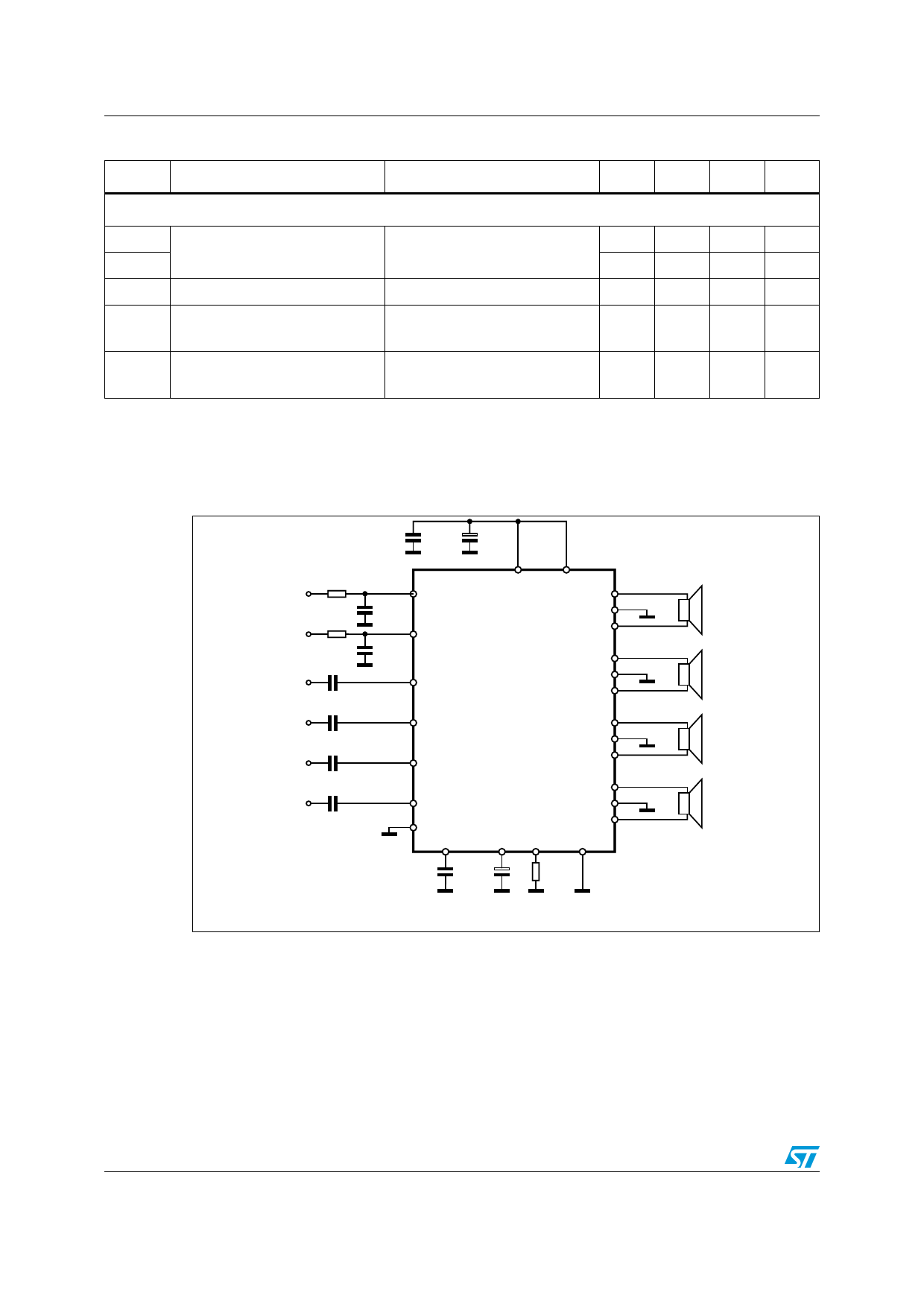
Standard test and application circuit, and PCB layout
Figure 3. Standard test and application circuit
34"9
-54%
).
2
+
2
+
#
M&
).
#�M&
).
#�M&
).
#�M&
#
M&
#
M&
#
M&
#
M&
6CC 6CC
3'.$
#
M&
362
#
M&
(3$/$ 4!"
2
�2�
�K7�TO�BE�PLACED�WHEN�PIN��IS�USED�AS�OFFSET�DETECTOR
/54
/54
/54
/54
'!0'03
8/17
Doc ID 6886 Rev 6
Share Link: 