AXK8L60125BG View Datasheet(PDF) - Panasonic Corporation
Part Name
Description
Manufacturer
AXK8L60125BG Datasheet PDF : 7 Pages
| |||
NOTES
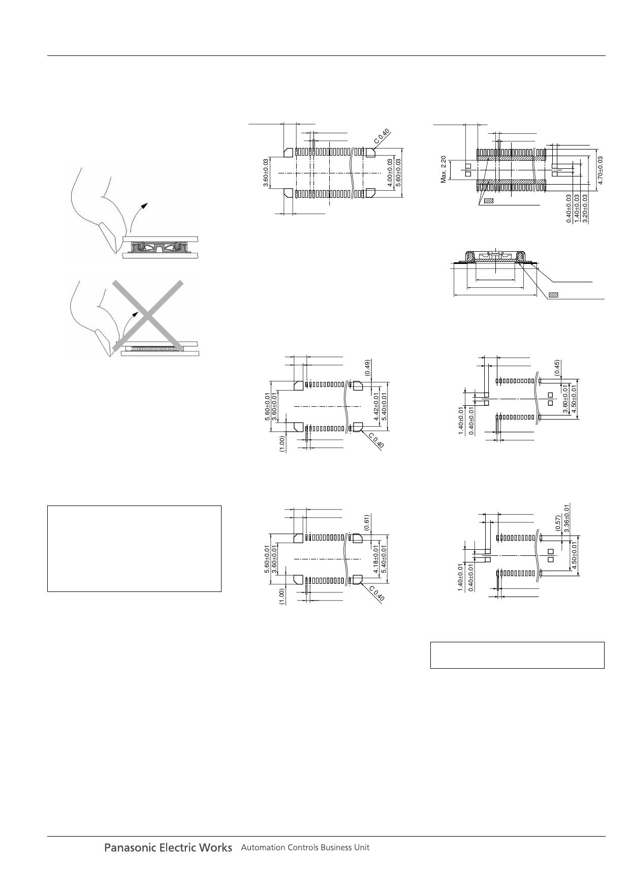
1. Removal by pulling up from an end
causes the entire connector removal
force to concentrate on the soldering
terminals and end terminals.
Therefore, please lift and remove from
the side. Doing so will also prevent
cracking of the soldered parts.
Socket
Recommended PC board pattern
(Mount pad arrangement pattern)
1.40±0.03
0.40±0.03
0.23±0.03
0.40
C
AXK7L, 8L
Header
Recommended PC board pattern
(Mount pad arrangement pattern)
1.40±0.03
0.40±0.03
0.23±0.03
0.57±0.03
NG
Pull
2. PC Boards and Recommended
Metal Mask Patterns
Connectors are mounted with high
density, with a pitch interval of 0.4 to 0.5
mm.
In order to reduce solder bridge and
other issues make sure the proper levels
of solder are used.
The figures to the right are recommended
metal mask patterns. Please use them as
a reference.
In particular, if a lot of solder is
used in the header retaining
soldering terminals, it might
interfere with and cause incomplete
socket mating. Therefore, please
follow the recommended
conditions give on the right.
1.00±0.03
: Insulation area
Relation between connector and mounting pad
Recommended metal mask pattern
Metal mask thickness: Here, 150 µm
(Terminal portion opening area ratio: 53 %)
(Metal portion opening area ratio: 100 %)
1.40±0.01
1.00±0.01
(Max. 2.20)
(3.20±0.03)
(4.70±0.03)
Mounting pad
: Insulation area
Recommended metal mask pattern
Metal mask thickness: Here, 150 µm
(Terminal portion opening area ratio: 52 %)
(Metal portion opening area ratio: 80 %)
1.40±0.01
0.46±0.01
0.20±0.01
0.40±0.01
C
0.40
Recommended metal mask pattern
Metal mask thickness: Here, 120 µm
(Terminal portion opening area ratio: 66 %)
(Metal portion opening area ratio: 100 %)
1.40±0.01
1.00±0.01
0.20±0.01
0.40±0.01
Recommended metal mask pattern
Metal mask thickness: Here, 120 µm
(Terminal portion opening area ratio: 66 %)
(Metal portion opening area ratio: 100 %)
1.40±0.01
0.57±0.01
0.20±0.01
0.40±0.01
C
0.40
0.20±0.01
0.40±0.01
For other details, please verify with
the product specification sheets.
panasonic-electric-works.net/ac
Share Link: 