MC33410FTA View Datasheet(PDF) - Motorola => Freescale
Part Name
Description
Manufacturer
MC33410FTA Datasheet PDF : 27 Pages
| |||
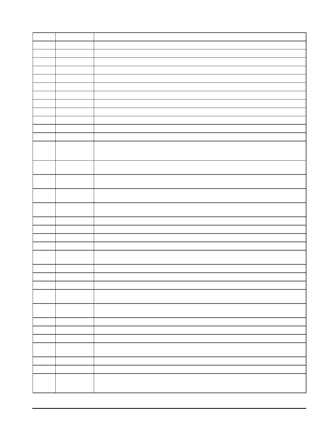
ÁÁÁÁÁÁPÁÁÁin ÁÁÁÁÁÁÁÁÁNamÁÁÁe ÁÁÁÁÁÁÁÁÁÁÁÁÁÁÁÁÁÁPÁÁÁINÁÁÁFUNÁÁÁCMTÁÁÁICO3NÁÁÁ3D4E1ÁÁÁS0CRÁÁÁIDPeTÁÁÁsIcOriNpÁÁÁtionÁÁÁÁÁÁÁÁÁÁÁÁÁÁÁÁÁÁÁÁÁÁÁÁÁÁÁÁÁÁÁÁÁÁÁÁ
1
FRx MC
Modulus Control Output to the Rx 64/65 or 128/129 dual modulus prescaler.
2
FRx
Input to the Rx PLL.
3
PLL VCC
Supply pin for the Rx PLL section. Allowable range is 2.7 to 5.5 V.
4
Rx PD
Phase detector charge pump output of the Rx PLL.
5
PLL Gnd
Ground pin for the PLL sections.
6
Tx PD
7
PLL VCC
8
FTx
9
FTx MC
10
EN
Phase detector charge pump output of the Tx PLL.
Supply pin for the Tx PLL section and the MPU Serial Interface section. Allowable range is 2.7 to 5.5 V.
Input to the Tx PLL.
Modulus Control Output to the Tx 64/65 or 128/129 dual modulus prescaler.
Enable input for the µP port. This signal latches in the register address and data.
11
CLK
Clock input for the µP port. Maximum frequency is 2.0 MHz.
12
Data
Bi–directional data line for the µP port. In Data Modem mode, this pin provides the recovered clock.
13
Status
Logic output which indicates that a predetermined 16 or 24–bit code word has been detected in the Data
Detect register, and the following data word has been loaded into register 10. In Data Modem mode, this
pin provides the Transmit Data clock.
14, 15
16
Fref In,
Fref Out
Low Battery/CD
A crystal, in the range of 4.0 to 18.25 MHz can be connected to these pins to provide the reference
frequency. If an external reference source is used, it is to be capacitively coupled to Fref In.
An open collector output. When low, indicates either the supply voltage (VCC) is low, or the carrier level is
above the threshold. This output is off when disabled.
17
Enc Out
18
VCC
m The digital output of the scrambler, which passes data from the CVSD encoder, or the Tx Data register, or
the Tx 1010 Generator. Source selection is done through the P port.
Supply input for the audio sections, filters, and CVSD blocks. Allowable range is 2.7 to 5.5 V. Internally
connected to Pins 27 and 37.
19
Enc In
The analog input to the CVSD encoder. Max. input level is 3.0 Vpp.
20
Tx Audio Out
Output of the transmit speech processing section.
21
Ground
Ground for the audio sections, filters, and CVSD blocks. Internally connected to Pins 30 and 40.
22
MCO
Output of the microphone amplifier, and input to the filters. This output has rail–to–rail capability.
23
MCI
Inverting input of the microphone amplifier. Gain and frequency response is set with external resistors and
capacitors.
24
Enc Cap
This capacitor sets the time constant for the CVSD encoder. This pin is sensitive to leakage.
25
VAG
Analog ground for the audio section and the CVSD encoder and decoder.
26
Dec Cap
The capacitor sets the time constant for the CVSD decoder. This pin is sensitive to leakage.
27
VCC
Supply input for the audio sections, filters, and CVSD blocks. Allowable range is 2.7 to 5.5 V. Internally
connected to Pins 18 and 37.
28, 29 PAO+, PAO–
Differential outputs of the power amplifier stage for driving an earpiece or hybrid network. The gain and
frequency response are set with external resistors and capacitors.
30
Gnd
Ground for the audio sections, filters, and CVSD blocks. Internally connected to Pins 21 and 40.
31
PAI
Input to the power amplifier stage. This pin is a summing node.
32
Rx Audio Output Output of the receive speech processing section.
33
VB
The capacitor filters the internal 1.5 V reference voltage. If VB is adjusted, it may be monitored at this pin.
m Max. load current is 10 A.
34
Rx Audio In
35
Dec Out
Input to the receive speech processing section.
The analog output of the CVSD decoder.
36
MP1
W As an output, provides the recovered Rx data, or the Data Detect output, or the data slicer output. Or it can
be set to a high impedance input (600 k ) for the carrier detect input signal. Selection is done through the
mP port. See Table 6.
NOTE: 1. All VCC pins must be within ±0.5 V of each other.
10
MOTOROLA RF/IF DEVICE DATA
Share Link: 