TC426 View Datasheet(PDF) - TelCom Semiconductor Inc => Microchip
Part Name
Description
Manufacturer
TC426 Datasheet PDF : 5 Pages
| |||
TC426
TC427
TC428
1.5A DUAL HIGH-SPEED
POWER MOSFET DRIVERS
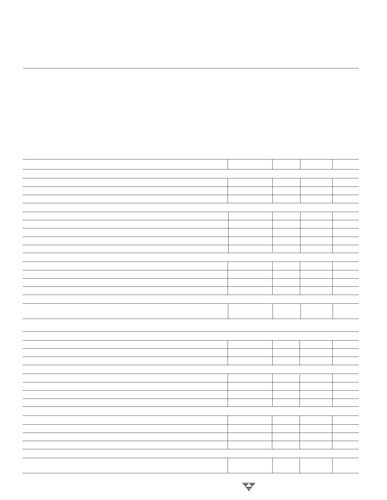
ABSOLUTE MAXIMUM RATINGS*
Supply Voltage ......................................................... +20V
Input Voltage, Any Terminal .... VDD + 0.3V to GND – 0.3V
Power Dissipation (TA ≤ 70°C)
Plastic ...............................................................730mW
CerDIP ..............................................................800mW
SOIC .................................................................470mW
Derating Factor
Plastic ............................................................. 8mW/°C
CerDIP ......................................................... 6.4mW/°C
SOIC ............................................................... 4mW/°C
Operating Temperature Range
C Version ................................................. 0°C to +70°C
I Version .............................................. – 25°C to +85°C
E Version ............................................ – 40°C to +85°C
M Version .......................................... – 55°C to +125°C
Maximum Chip Temperature ................................. +150°C
Storage Temperature Range ................ – 65°C to +150°C
Lead Temperature (Soldering, 10 sec) ................. +300°C
ELECTRICAL CHARACTERISTICS: TA = +25°C with 4.5V ≤ VDD ≤ 18V, unless otherwise specified.
Symbol
Parameter
Test Conditions
Min
Typ
Max
Unit
Input
VIH
Logic 1, High Input Voltage
VIL
Logic 0, Low Input Voltage
IIN
Input Current
Output
VOH
High Output Voltage
VOL
Low Output Voltage
ROH
High Output Resistance
ROL
Low Output Resistance
IPK
Peak Output Current
Switching Time (Note 1)
tR
Rise Time
tF
Fall Time
tD1
Delay Time
tD2
Delay Time
Power Supply
IS
Power Supply Current
0V ≤ VIN ≤ VDD
IOUT = 10 mA, VDD = 18V
IOUT = 10 mA, VDD = 18V
Test Figure 1/2
Test Figure 1/2
Test Figure 1/2
Test Figure 1/2
VIN = 3V (Both Inputs)
VIN = 0V (Both Inputs)
2.4
—
—
—
–1
—
VDD – 0.025
—
—
—
—
10
—
6
—
1.5
—
—
—
—
—
—
—
—
—
—
—
—
—
0.8
1
—
0.025
15
10
—
30
30
50
75
8
0.4
V
V
µA
V
V
Ω
Ω
A
nsec
nsec
nsec
nsec
mA
mA
ELECTRICAL CHARACTERISTICS: Over Operating Temperature Range with 4.5V ≤ VDD ≤ 18V, unless otherwise specified.
Input
VIH
VIL
IIN
Output
Logic 1, High Input Voltage
Logic 0, Low Input Voltage
Input Current
0V ≤ VIN ≤ VDD
2.4
—
—
V
—
—
0.8
V
–10
—
10
µA
VOH
High Output Voltage
VDD – 0.025
—
—
V
VOL
Low Output Voltage
—
—
0.025
V
ROH
High Output Resistance
IOUT = 10 mA, VDD = 18V
—
13
20
Ω
ROL
Low Output Resistance
IOUT = 10 mA, VDD = 18V
—
8
15
Ω
Switching Time (Note 1)
tR
tF
tD1
tD2
Power Supply
Rise Time
Fall Time
Delay Time
Delay Time
Test Figure 1/2
Test Figure 1/2
Test Figure 1/2
Test Figure 1/2
—
—
60
nsec
—
—
30
nsec
—
—
75
nsec
—
—
120
nsec
IS
Power Supply Current
NOTE: 1. Switching times guaranteed by design.
VIN = 3V (Both Inputs)
VIN = 0V (Both Inputs)
—
—
12
mA
—
—
0.6
mA
4-170
TELCOM SEMICONDUCTOR, INC.
Share Link: 