CS8151YDPSR7G(2008) View Datasheet(PDF) - ON Semiconductor
Part Name
Description
Manufacturer
CS8151YDPSR7G
(Rev.:2008)
(Rev.:2008)
ON Semiconductor

CS8151YDPSR7G Datasheet PDF : 14 Pages
| |||
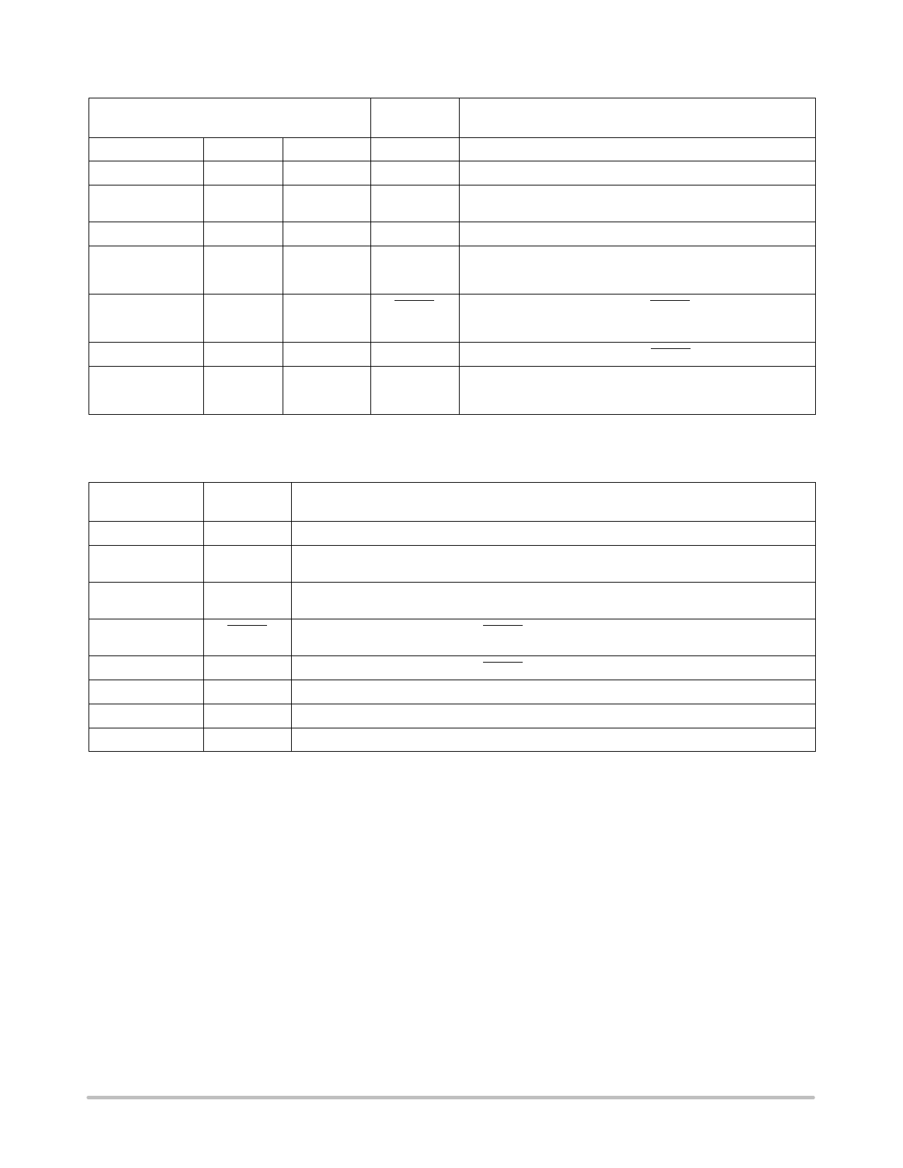
CS8151
PACKAGE PIN DESCRIPTION
Package Pin #
SO−14L
D2PAK
SO−16L
7
1
8
8
2
9
9
3
11
Pin
Symbol
VOUT
VIN
WDI
Function
Regulated output voltage 5.0 V ± 2%.
Supply voltage to the IC.
CMOS/TTL compatible input lead. The Watchdog function monitors the falling
edge of the incoming signal.
3−5,
10−12
4
4, 5, 6, 12, 13* GND Ground connection.
13
5
14
Wake Up CMOS/TTL compatible output consisting of a continuously generated signal used
to Wake Up the microprocessor from sleep mode.
14
6
15
RESET CMOS/TTL compatible output lead RESET goes low whenever VOUT drops by
more than 6.0% from nominal, or during the absence of a correct watchdog
signal.
1
7
16
Delay Input lead from timing capacitor for RESET and Wake Up signal.
6
−
7
Sense Kelvin connection which allows remote sensing of the output voltage for im-
proved regulation. If remote sensing is not required, connect to VOUT.
*Pin 6 GND is not directly shorted to the fused paddle GND. The fused paddle GND (pins 4, 5, 12, 13) is connected through the substrate.
Pin 6 must be electrically connected to at least one of the fused paddle GND’s on the PC board.
http://onsemi.com
5
Share Link: