CS8151YDPS7 View Datasheet(PDF) - ON Semiconductor
Part Name
Description
Manufacturer
CS8151YDPS7
ON Semiconductor

CS8151YDPS7 Datasheet PDF : 16 Pages
| |||
CS8151
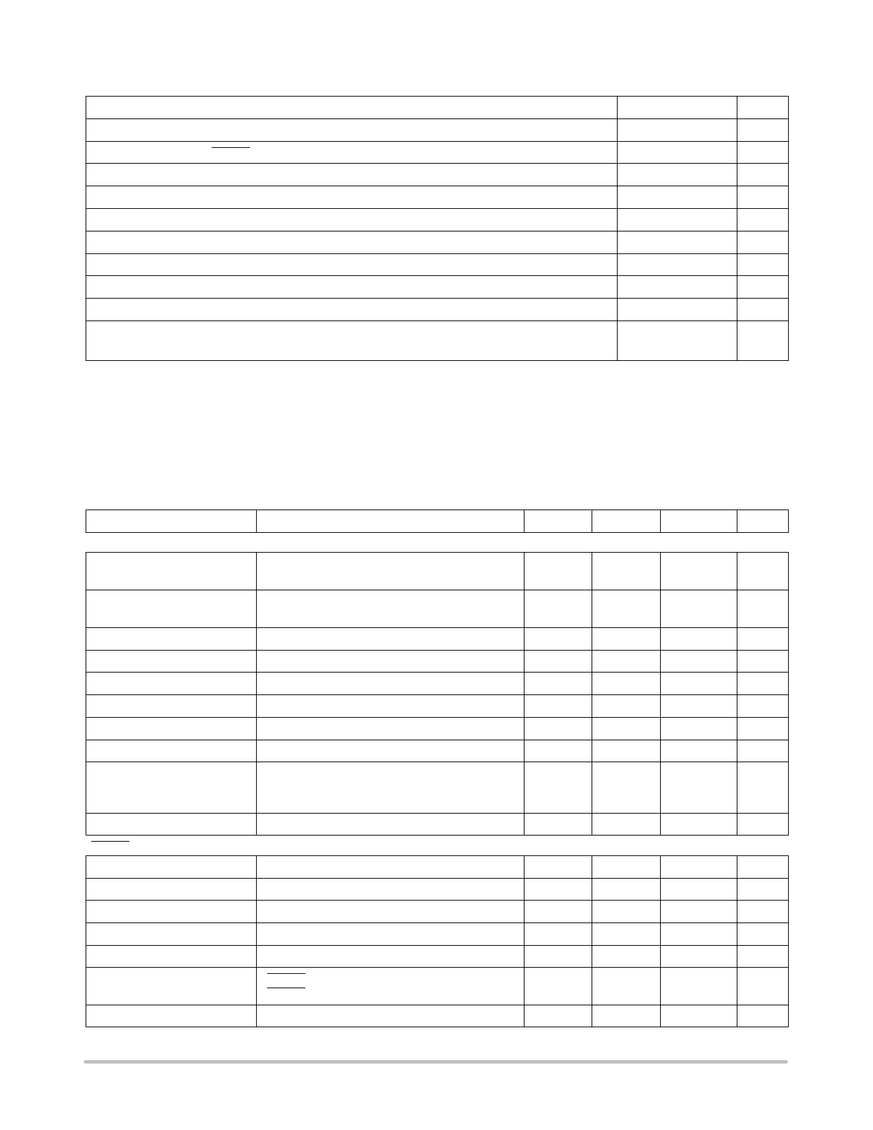
MAXIMUM RATINGS*
Power Dissipation
Rating
Value
Unit
Internally Limited
−
Output Current (VOUT, RESET, Wake Up)
Reverse Battery
Internally Limited
−
−15
V
Peak Transient Voltage (60 V Load Dump @ VIN = 14 V)
Maximum Negative Transient (t < 2.0 ms)
+74
V
−50
V
ESD Susceptibility (Human Body Model)
2.0
kV
ESD Susceptibility (Machine Model)
200
V
Logic Inputs/Outputs
−0.3 to +6.0
V
Storage Temperature Range
−55 to +150
°C
Lead Temperature Soldering
Wave Solder (through hole styles only) (Note 1)
260 peak
°C
Reflow (SMD styles only) (Notes 2 & 3)
240 peak
°C
Maximum ratings are those values beyond which device damage can occur. Maximum ratings applied to the device are individual stress limit
values (not normal operating conditions) and are not valid simultaneously. If these limits are exceeded, device functional operation is not implied,
damage may occur and reliability may be affected.
1. 10 seconds max
2. 60 seconds max above 183°C
3. −5°C / +0°C allowable conditions
*The maximum package power dissipation must be observed
ELECTRICAL CHARACTERISTICS (−40°C ≤ TA ≤ 125°C, −40°C ≤ TJ ≤ 150°C, 6.0 V ≤ VIN ≤ 26 V, 100 mA ≤ IOUT ≤ 100 mA,
C2 = 47 mF (ESR < 8.0 W), CDelay = 0.1 mF; unless otherwise specified.)
Characteristic
Test Conditions
Min
Typ
Max
Unit
Output Section
Output Voltage, VOUT
9.0 V < VIN < 16 V
6.0 V < VIN < 26 V, 0 < IOUT < 100 mA
4.90
5.0
4.85
5.0
5.10
V
5.15
V
Dropout Voltage (VIN − VOUT)
IOUT = 100 mA
IOUT = 100 mA
−
400
600
mV
−
100
150
mV
Load Regulation
Line Regulation
Ripple Rejection
Current Limit
Thermal Shutdown
VIN = 14 V, 100 mA < IOUT < 100 mA
−
10
IOUT = 1.0 mA, 6.0 V < VIN < 26 V
−
10
7.0 V < VIN < 17 V @ f = 120 Hz, IOUT = 100 mA
60
75
VOUT = 4.5 V
100
250
−
150
180
50
mV
50
mV
−
dB
−
mA
210
°C
Overvoltage Shutdown
Quiescent Current
VOUT < 1.0 V
IOUT = 200 mA (Sleep)
IOUT = 50 mA
IOUT = 100 mA (Wake Up)
50
56
62
V
−
0.4
0.75
mA
−
4.0
−
mA
−
12
20
mA
Reverse Current
RESET
VOUT = 5.0 V, VIN = 0 V
−
1.0
1.5
mA
Threshold High (RTH)
Threshold Low (RTL)
Hysteresis
RTH VOUT Increasing
RTL VOUT Decreasing
RTH − RTL
VOUT − 0.3
−
4.5
4.7
150
200
VOUT − 0.04
V
4.91
V
250
mV
Output Low
Output High
Current Limit
1.0 V < VOUT RTL, IOUT = 25 mA
IOUT = 25 mA, VOUT > RTH
RESET = 0 V, VOUT > VRTH (Sourcing)
RESET = 5.0 V, VOUT > 1.0 V (Sinking)
−
0.2
3.8
4.2
0.025
0.5
0.1
12
0.8
V
5.1
V
1.30
mA
80
mA
Delay Time
POR Mode
3.0
5.0
7.0
ms
http://onsemi.com
3
Share Link: