CXD1961Q View Datasheet(PDF) - Sony Semiconductor
Part Name
Description
Manufacturer
CXD1961Q Datasheet PDF : 15 Pages
| |||
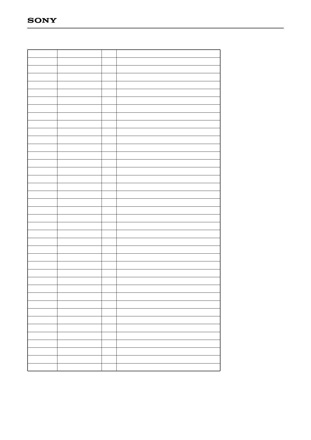
Pin Description
No.
1
2
3
4
5
6
7–9
10
11
12
13
14
15
16
17
18
19
20
21
22
23
24
25
26
27
28
29–33
34
35
36–38
39–43
44
45
46–48
49
50
51
52
53
54
Symbol
AVS0
RB0
VDD0
VSS0
CPUSEL
PLLSEL
TEST1–3
VDD1
VSS1
SDATA
SCLK
SEN
VDD2
VSS2
TCK
TMS
TDO
TDI
CK8OUT
RESET
TE
VDD3
VSS3
PKTCLK
BYTCLK
PKTERR
DATA0–4
VDD4
VSS4
DATA5–7
D0–D4
VDD5
VSS5
D5–D7
RW
DS
CS
ADD0
VDD6
VSS6
I/O
Description
— Analog Ground
— ADC0 bottom reference voltage
— Digital Power Supply (+3.3 V)
— Digital Ground
I CPU interface select (L : I2C bus)
I Connect Digital Ground
I Test input (connect Digital Ground)
— Digital Power Supply (+3.3 V)
— Digital Ground
O SONY internal use
O SONY internal use
O SONY internal use
— Digital Power Supply (+3.3 V)
— Digital Ground
I JTAG test clock
I JTAG test mode select
O JTAG test data output
I JTAG test data input
O Divide by 8 clock of Crystal clock
I Reset input (L : reset)
I Test Enable (H : test enable)
— Digital Power Supply (+3.3 V)
— Digital Ground
O R/S Packet clock
O R/S Byte clock
O R/S uncorrectable Packet flag
O R/S data output (DATA0 : LSB)
— Digital Power Supply (+3.3 V)
— Digital Ground
O R/S data output (DATA7 : MSB)
I/O 8 bit CPU bus data I/O (D0 : LSB)
— Digital Power Supply (+3.3 V)
— Digital Ground
I/O 8 bit CPU bus data I/O (D7 : MSB)
I 8 bit CPU bus Read/Write (H : Read)
I 8 bit CPU bus Data strobe
I 8 bit CPU bus Chip Select
I 8 bit CPU bus Address0 (LSB)
— Digital Power Supply (+3.3 V)
— Digital Ground
—4—
CXD1961Q
Share Link: 