CXD1961Q View Datasheet(PDF) - Sony Semiconductor
Part Name
Description
Manufacturer
CXD1961Q Datasheet PDF : 15 Pages
| |||
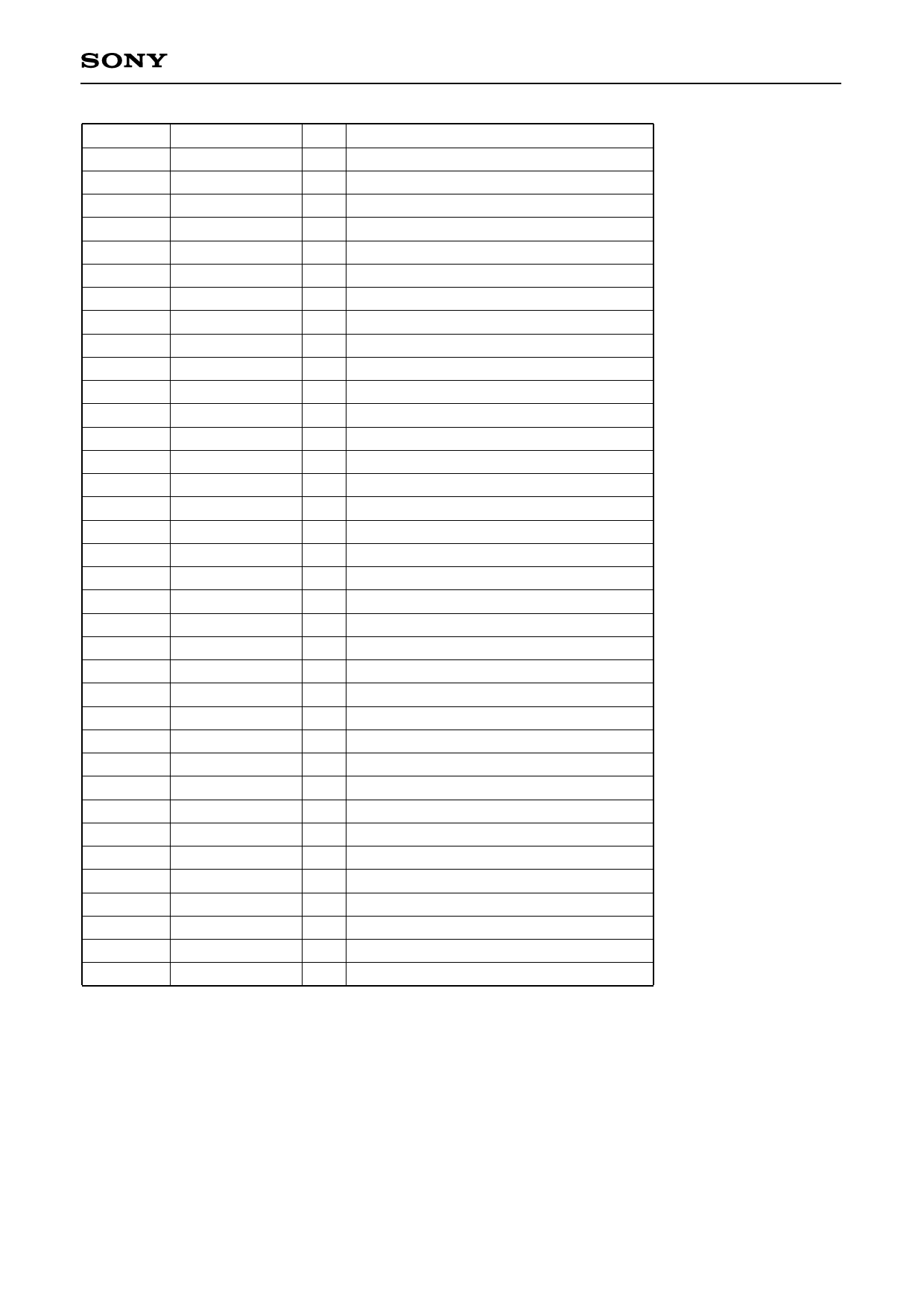
No.
Symbol
I/O
Description
55–57
ADD1–3
I 8 bit CPU bus Address1–3 (ADD3 : MSB)
58
SCL
I I2C bus serial clock
59
SDA
I/O I2C bus serial data
60
VDD7
— Digital Power Supply (+3.3 V)
61
VSS7
— Digital Ground
62
XO
O Oscillator output (for Crystal)
63
XI
I Oscillator input (for Crystal)
64, 65
TEST4, 5
O Test output (VSS level)
66
VDD8
— Digital Power Supply (+3.3 V)
67
VSS8
— Digital Ground
68
AGCPWM
O PWM output for AGC
69
CKV
O Sampling Clock monitor output
70–73
CR0–3
O Clock Recovery data 0–3 (CR0 : LSB)
74
VDD9
— Digital Power Supply (+3.3 V)
75
VSS9
— Digital Ground
76–79
CR4–7
O Clock Recovery data 4–7 (CR7 : MSB)
80
VDD10
— Digital Power Supply (+3.3 V)
81
VSS10
— Digital Ground
82, 83
TEST6, 7
O Test output (VSS level)
84
VDD11
— Digital Power Supply (+3.3 V)
85
VSS11
— Digital Ground
86
CPOUT
O PLL Charge pump output
87
AVD2
— Analog Power Supply (+3.3 V)
88
VCOC
I VCO control voltage input
89
OPXIN
I Embedded OP-Amp Negative input
90
OPOUT
O Embedded OP-Amp output
91
AVS2
— Analog Ground
92
VCOEN
I VCO enable (H : enable)
93
RT1
— ADC1 top reference voltage
94
AVD1
— Analog Power Supply (+3.3 V)
95
QIN
I Analog Q input (ADC1 input)
96
AVS1
— Analog Ground
97
RB1
— ADC1 bottom reference voltage
98
RT0
— ADC0 top reference voltage
99
AVD0
— Analog Power Supply (+3.3 V)
100
IIN
I Analog input (ADC0 input)
Note)
Apply 0.1 µF capacitor to every power supply terminal.
Apply 0.1µF capacitor to RB0, RT0, RB1, RT1 for stable A to D conversion.
CXD1961Q
—5—
Share Link: 