CXD1961Q View Datasheet(PDF) - Sony Semiconductor
Part Name
Description
Manufacturer
CXD1961Q Datasheet PDF : 15 Pages
| |||
CXD1961Q
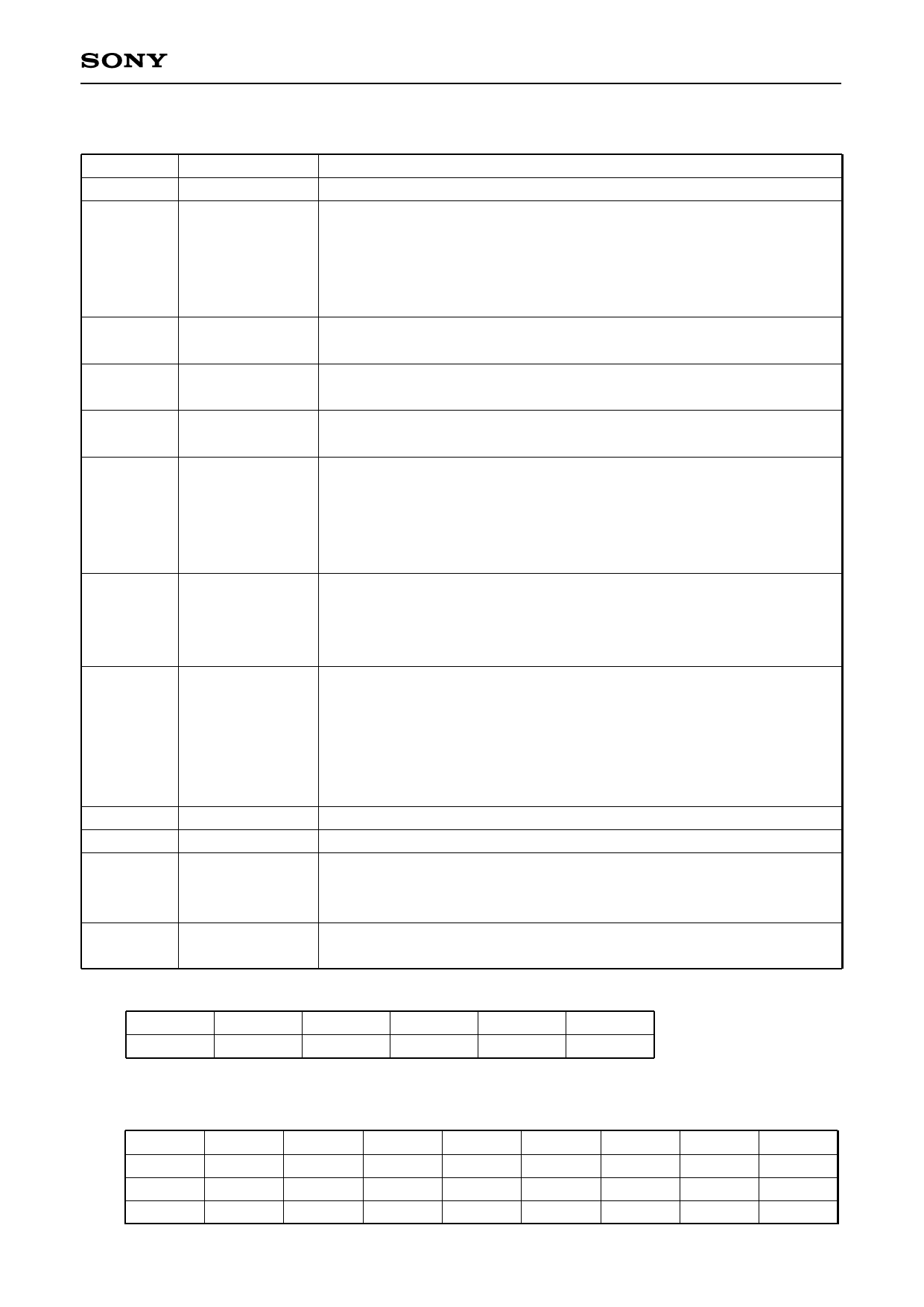
CPU Interface Register Brief Explanation
ADD 0
ADD 1, 2
ADD 3
ADD 4
ADD 5
ADD 6
ADD 7
ADD 8
ADD 9
ADD A
ADD A, B, C
ADD C
ADD D, E, F
ADC_IN (7 : 0) ADC input level (I2+Q2 at QPSK demodulator)
BECNT (15 : 0) Bit Error Count at QPSK demodulator output
QSYNC
QPSK Synchronization Flag (H : in sync.)
AFC (3 : 0)
Auto Frequency Control data
VSYNC
Viterbi dec. Synchronization Flag (H : in sync)
RSYNC
Reed-Solomon dec. Synchronization Flag (H : in sync)
BEM_END
Bit Error Monitor enable Flag (H : enable)
AGC (7 : 0)
(when AGC mode is H) AGC Gain control data
(when AGC mode is L) Reference data for self AGC
VS_N (4 : 0)
V sync threshold Bit Error Count (see Fig. 1)
RATE (2 : 0)
Punctured rate (see Fig. 2)
QS_N (3 : 0)
Threshold data for QPSK sync. judgement (see Fig. 3)
AC (2 : 1), BC (2 : 1) Parameter for Carrier recovery loop filter (see Fig. 4)
AK (2 : 1)
Parameter for Clock recovery loop filter (see Fig. 4)
S_INV
I/Q exchange (H : enable)
AGC_INV
AGC control voltage polarity (H : positive)
AGC_MOD
H : controlled by CPU (slave) L : self AGC mode (master)
TIMER (2 : 0)
Timer for AGC master mode (see Fig. 5)
PLL_CTL
For SONY internal use (input 0 for norma use)
MON_SW
For SONY internal use (input 0 for norma use)
VS_T (3 : 0)
Monitor period for Viterbi sync. (see Fig. 6)
CE_LEV (1 : 0) Clock recovery Error feed back level (see Fig. 7)
DF_SKIP
Digital Filter skip mode (H : enable)
DOUT_INV
Data output timing invert (H : falling edge)
RS_SKIP
R/S decode skip mode (H : enable)
SSEL
For SONY internal use (input 0 for normal use)
AFC_MOD
For SONY internal use (input 0 for normal use)
BER_T (2 : 0)
Monitor period for Bit error Count (see Fig. 8)
HS_PLL
For SONY internal use (input 0 for normal use)
SFD (17 : 11)
For SONY internal use (input 0 for normal use)
PCD (2 : 0)
For SONY internal use (input 0 for normal use)
REF_SEL
For SONY internal use (input 0 for normal use)
REF_LSB
For SONY internal use (input 0 for normal use)
NC0 (23 : 0)
Sampling Frequency 2*Fs=NC0 (0 : 23)*8*Fxtal/224
(Fxtal=Crystal Frequency)
Fig. 1 V sync threshold (Error Counter Preset data)
Register VS_N4 VS_N3 VS_N2 VS_N1 VS_N0
Limit
×29
×28
×27
×26
×25
(ex. VS_N (4 : 0)=(1, 1, 0, 0, 1) Limit=0×29+0×28+1×27+1×26+0×25=192)
max. : 992
min. : 32
Fig. 2 Punctured Rate
Punc. rate 1/2
2/3
3/4
4/5
5/6
6/7
7/8
RATE2
0
0
0
1
1
1
1
RATE1
0
1
1
0
0
0
1
RATE0
1
0
1
0
1
0
1
—7—
Auto
0
0
0
Share Link: 