AD9100(RevA) View Datasheet(PDF) - Analog Devices
Part Name
Description
Manufacturer
AD9100 Datasheet PDF : 12 Pages
| |||
AD9100
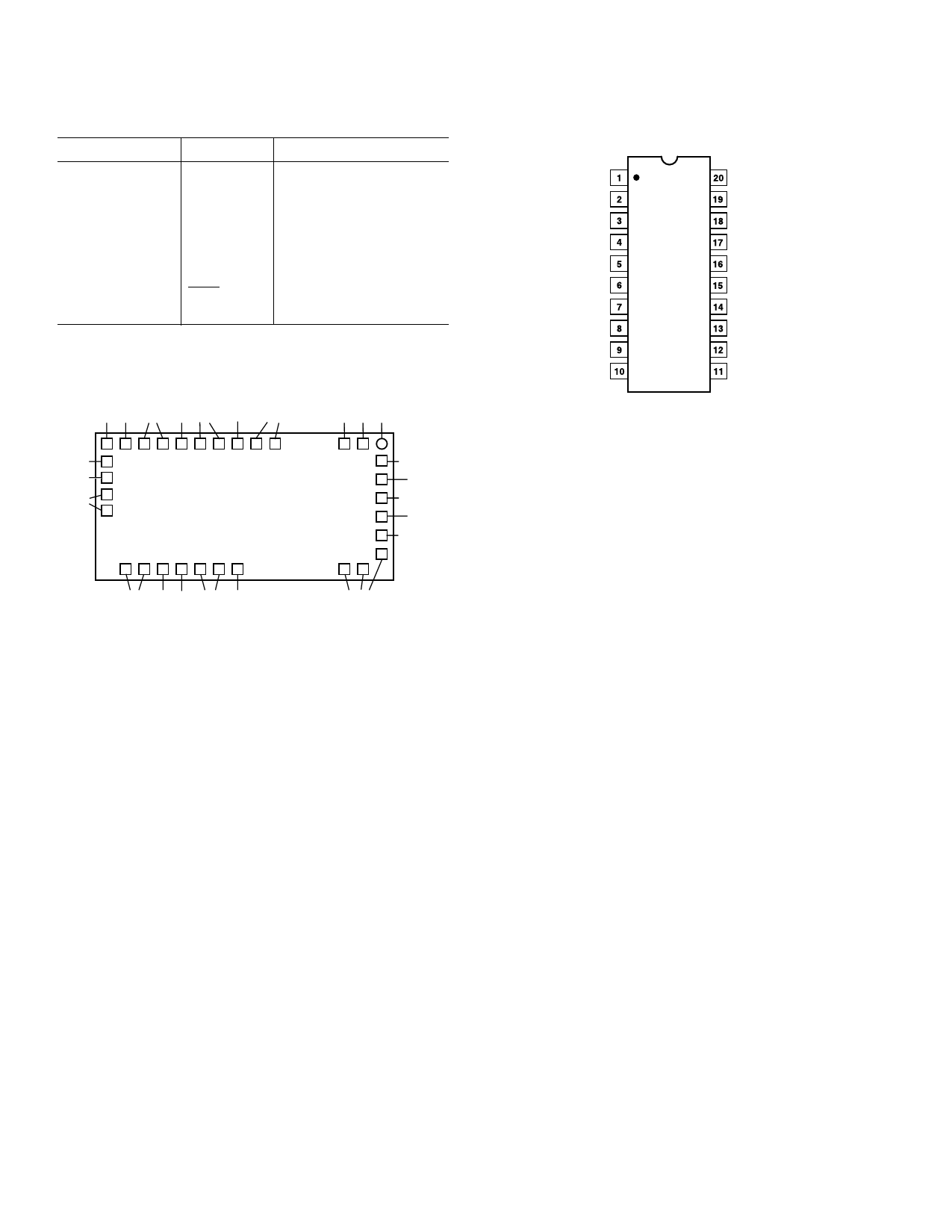
DIP PIN DESCRIPTIONS/CONNECTIONS
LCC PIN DESCRIPTIONS/CONNECTIONS
Pin No.
Description Connection
Pin No.
Description Connection
1
–VS
–5.2 V Power Supply
l
GND
Common Ground Plane
2
GND
Common Ground Plane
2
GND
Common Ground Plane
3
GND
Common Ground Plane
3
NC
None
4
VIN
Analog Input Signal
4
–VS
–5.2 V Power Supply
5
–VS
–5.2 V Power Supply
5
–VS
–5.2 V Power Supply
6
BYPASS
0.1 µF to Ground
6
NC
None
7
–VS
–5.2 V Power Supply
7
VIN
Analog Input Signal
8
GND
Common Ground Plane
8
–VS
–5.2 V Power Supply
9
VOUT
Track-and-Hold Output
9
–VS
–5.2 V Power Supply
10
GND
Common Ground Plane
10
NC
None
OBSOLETE 11
GND
Common Ground Plane
11
12
GND
Common Ground Plane
12
13
GND
Common Ground Plane
13
14
+VS
+5 V, Power Supply
14
15
BYPASS
0.1 µF to Ground
15
16
+VS
+5 V, Power Supply
16
17
GND
Common Ground Plane
17
18
CLK
Complement ECL Clock
18
19
CLK
“True” ECL Clock
19
20
+VS
+5 V Power Supply
20
21
22
23
–VS 1
20 +VS
24
GND 2
19 CLK
25
GND 3
18 CLK
26
27
VIN 4
–VS 5
17 GND
AD9100 16 +VS
28
–VS
–VS
–VS
BYPASS
VOUT
BYPASS
+VS
+VS
+VS
HOLDCAP
HOLDCAP
+VS
+VS
GND
+VS
+VS
CLOCK
CLOCK
–5.2 V Power Supply
–5.2 V Power Supply
–5.2 V Power Supply
0.1 µF to Pin 16
Track-and-Hold Output
0.1 µF to Pin 14
+5 V Power Supply
+5 V Power Supply
+5 V Power Supply
External Hold Capacitor
External Hold Capacitor
+5 V Power Supply
+5 V Power Supply
Common Ground Plane
+5 V Power Supply
+5 V Power Supply
Complement ECL Clock
“True” ECL Clock
TOP VIEW
BYPASS 6 (Not to Scale) 15 BYPASS
–VS 7
GND 8
14 +VS
13 GND
VOUT 9
12 GND
26 27 28 1 2 3 4
GND 10
11 GND
CHIP PAD ASSIGNMENTS
+VS +VS
+VS CAP HOLD CAP
NC GND +VS (NOTE 1) (NOTE 3)
+VS +VS NC
CLOCK
CLOCK
GND
12 11 10 9 8 7 6 5 4
14
15
16
AD9100
17
TOP VIEW
(Not to scale)
18 19 20 21 22 23 24
32
32
31
30
29
28
25 26
+VS
BYPASS
(NOTE 2)
+VOUT
BYPASS
(NOTE 2)
+VS
+VS 25
GND 24
+VS 23
+VS 22
HOLDCAP 21
HOLDCAP 20
PINS
+VS 19
20, 21
22pF
(CH)
AD9100
BOTTOM VIEW
(Not to Scale)
18 17 16 15 14 13 12
NC = NO CONNECT
5 –VS
6 NC
7 VIN
8 –VS
9 –VS
10 NC
11 –VS
PIN 14
PIN 16
0.01µF LOW
INDUCTANCE
Pad Name
Pad Name
Pad Name
–VS NC –VIN –VS –VS CAP
–VS
(NOTE 1)
SIZE = 148 × 63 × 15 mils NC = NO CONNECT
NOTES:
1. SUPPLY BYPASS CAPACITOR; 0.01 TO 0.1µF CERAMIC
CONNECTED TO GROUND.
2. 0.01µF CERAMIC CONNECTED BETWEEN PAD 29 AND PAD 31.
3. HOLD CAPACITOR CONNECTED FROM PAD 4 AND PAD 5 TO
GROUND; 10–100pF, NOMINALLY 22pF. DIP PACKAGE DOES NOT
REQUIRE EXTERNAL HOLD CAPACITOR.
1 NC
12 +VS
23 –VS
2
+VS
13 +VS
24
–VS CAP1
3
+VS
14 CLOCK 25 –VS
4 HOLDCAP3 15 CLOCK 26 –VS
5 HOLDCAP3 16 GND
27 –VS
6
+VS CAP1
17 GND
28 +VS
7
+VS
18 –VS
29 BYPASS2
8
+VS
19 –VS
30
VOUT
9 GND
20 NC
31 BYPASS2
10 NC
11 NC
21
VIN
22 –VS
32 +VS
–4–
REV. A
Share Link: 